This is the first of a series of blog postings describing my latest
homebrew project -- a 500 watt HF Power Amplifier:
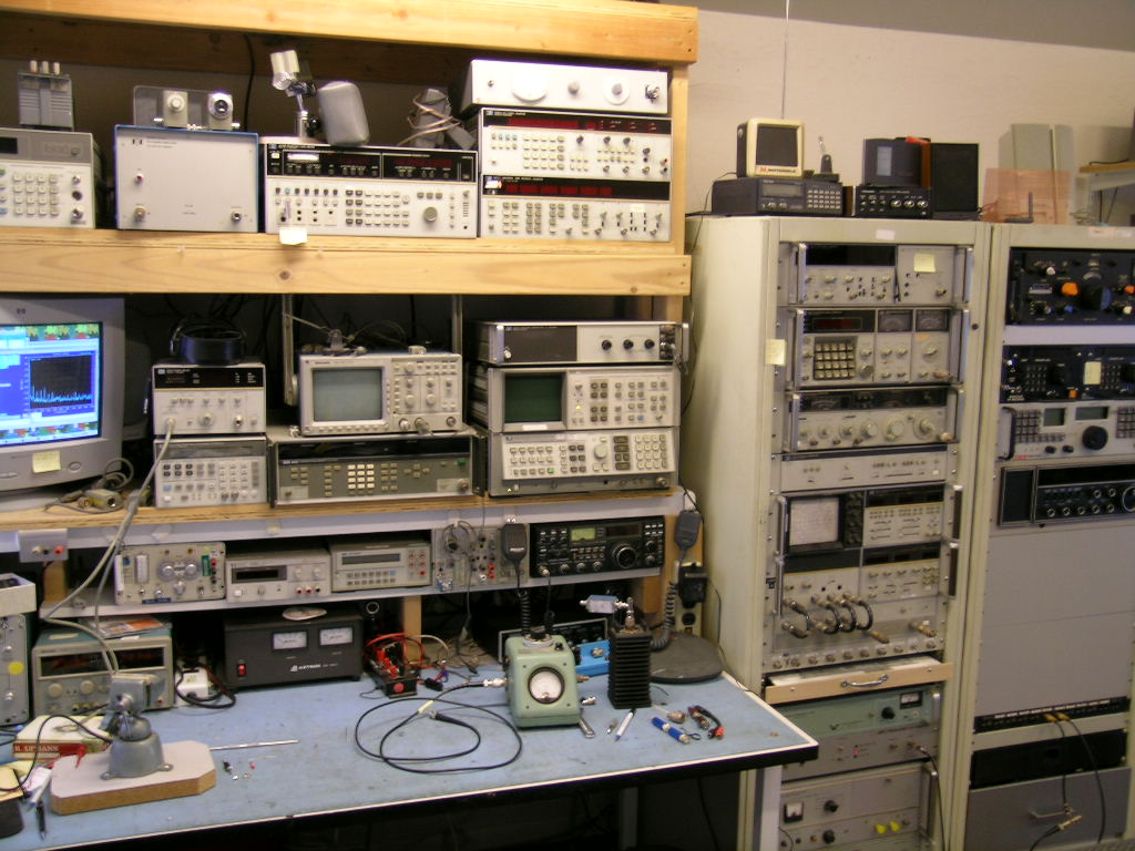
I started this project back in 2016 -- I had finished my Automatic Antenna Tuner (seen in the upper-left of the picture, above) and a PA project seemed like the ideal next step.
While researching RF amplifiers, I discovered a Microsemi App Note, "A 700W Broadband Amplifier using VRF2944". I decided to use its design as the basis of my PA and began gathering parts.
But, as is typical for me, the path forward for a new project is rarely straight. While I was gathering parts for this PA project a friend, Dick Benson, W1QG, convinced me to work on his FPGA SDR project. I was intrigued by the concept and decided to explore it further, and so I put the PA project aside and built an FPGA-based HF transceiver (seen in the upper-right of the picture, above)
The PA project lay fallow until earlier this year when I decided to resurrect it. Finishing it took the better part of the remaining year, but now it is done! This series of blog posts describes the design (should others find my it, or my experiences, useful) and is also a repository for my notes.
Finally, I will note -- this is my first PA project, so I am very much a novice when it comes to the intricacies of PA design. There's a heck of a lot I do not know, and I'm sure it will show in these blog posts.
With that caveat out of the way, let's get started...
Preliminary Design Goals:
My preliminary design goals were, when operating into a 50 ohms load:
1. 500 watts out, minimum, on 80 - 10 meters. This excludes 60 meters due to its 100 watt radiated power limitation, and I decided to skip 160 and 6 meters because I never operate on those bands.
2. Two-tone Intermodulation Distortion Products at least 30 dB down from the level either of the two tones.
Why at least 30 dB? Per the chapter "Solid-state Power Amplifiers" in the book, Single Sideband Systems and Circuits, Second Edition, (edited by William E. Sabin and Edgar O. Schoenike, both of Collins Radio),"this is a typical specification for good-quality, commercial, high-power HF PAs."
The author of the chapter adds that "typical amateur-grade solid-state PA specifications range from -30 dB to as poor as -20 dB below one of two equal tones."
So why not strive to at least equal a "good-quality, commercial" PA?
Note that the chapter's author defines IMD relative to the level of one of the two equal tones. The ARRL does not measure two-tone IMD relative to the level of either of the tones (i.e. measured in "dBc", per this article: Two-tone IMD Measurement Techniques). Instead, they measure IMD with respect to the PEP level which, when the test signal consists of two tones of equal amplitude, is 6 dB above the level of either of the two tones. I.e:
Thus, two-tone IMD product measurements made with the ARRL method will appear more optimistic by 6 dB, compared to measurements made referencing the two-tone products against the level of either of the two tones (i.e. the latter measured as dBc).
Below is a table of ARRL two-tone IMD test results (taken from QST) whose entries I've converted to dBc by subtracting 6 dB from the values published in QST (i.e. they are now referenced to the level of either tone, not referenced to PEP).
The yellow-highlighted rows are 500W amps. And the "amber" cells highlight the 500W amps whose two-tone IMD products do not meet my 30 dB-minimum IMD-product (dBc) requirement.
Note that almost every 500W amplifier on the list fails this specification! I would discover that trying to achieve it would be a major headache! But more on this in my next blog post...
3. Harmonic Distortion at least 43 dB down from the fundamental carrier.
To quote the relevant FCC spec (CFR Title 47, Chapter I, Subchapter D, Part 97, Subpart D, Section 97.307) (I've highlighted the important part).
§ 97.307 Emission standards.
(d) For transmitters installed after January 1, 2003, the mean power
of any spurious emission from a station transmitter or external RF power amplifier transmitting on a frequency below 30 MHz must be at least 43 dB below the mean power of the fundamental
emission. For transmitters installed on or before January 1, 2003, the mean
power of any spurious emission from a station transmitter or external RF power amplifier transmitting on a frequency below 30 MHz must not exceed 50 mW
and must be at least 40 dB below the mean power of the fundamental
emission. For a transmitter of mean power less than 5 W installed on or
before January 1, 2003, the attenuation must be at least 30 dB. A
transmitter built before April 15, 1977, or first marketed before
January 1, 1978, is exempt from this requirement.
4. Input Impedance. SWR of 1.5:1 or better.
5. Power Source 120 VAC (nominal).
Block Diagram:
Here is a block diagram of my 500W HF PA:
Notes on this Block Diagram:
1. The RF path starts at the rear-panel input with a BNC connector. It then goes to the T/R switch which, when the amplifier is engaged in Transmit mode, routes the RF to the amplifier, otherwise the T/R switch connects the input BNC directly to the output N connector, bypassing the amp.
2. When the amplifier is Transmitting, the RF is routed to the Amplifier Assembly's input. This assembly's output then goes to the Low Pass Filter (LPF) Assembly via a Directional Coupler, the latter verifies if the LPF assembly is operating correctly: if the SWR at the input of the LPF is more than about 3:1, a fault is declared and the PA shuts down (more on this in a later blog post).
The advantage of such a circuit is described in the "A New 250-W Broadband Linear Amplifier" design in the 2011 ARRL Handbook for Radio Communications (section 17.11). (It is probably in other Handbooks, too). And interestingly, the designer of this Handbook amp is also the designer of the 700W Microsemi App-Note amp that is the foundation of my project.
A similar "low-pass filter error" function can be found on W6PQL's website (here). I've adapted his design to my PA, with some small changes.
Also, the LPF circuit is essentially the W6PQL LPF design, with some small changes.
3. From the Low Pass Filter Assembly the RF goes back to the T/R switch and then on to the output Directional Coupler Assembly, which measures the output power and the output SWR. (This assembly also creates an "RF Sample" signal that is 50 dB down from the RF output signal -- for signal monitoring purposes -- but this signal is not shown on the block diagram).
4. The PA is designed to be controlled primarily by a parallel interface from my FPGA-SDR transceiver ((via an RG-45 connector -- see here and here for the schematics of this interface on the transceiver side of the link). This interface allows me to automatically select the appropriate PA low-pass filter as I change bands on the transceiver.
But there is also a more traditional RCA jack on the back panel to control the PA's T/R if using some other transceiver or transmitter/receiver combo. In this case the appropriate LPF filter would be selected manually, rather than automatically, via the PA's front-panel controls.
5. The PA's Vdd voltage is about 62.5VDC (shown as 62V on the block diagram). This voltage comes from two commercial 27V switchers, connected in series, whose outputs have each been adjusted to their max of about 31V.
6. The Controller Assembly is the PA's control circuitry. It does the following:
- Handles T/R Switching (via Interrupt control), nesting PA bias On/Off within the T/R relay switchover (so that the PA is not ON while the TR relay is switching).
- Monitors the levels of various analog signals: Vdd, Idd, PoutFwd, PoutRef, PA Temperature.
- Monitors Fault Conditions and shuts off Vdd and Bias Voltage to PA Assembly if certain faults are detected.
- Monitors Front Panel Controls.
- Controls the LCD Display and the Analog RF Power Meter's reading.
- Monitors PA Heatsink Temperature and adjusts Fan Speed accordingly.
- Selects the appropriate Low-pass Filter.
The Arduino also calculates Forward Power and SWR, and displays these values, as well as Vdd, Idd, and the temperature of the PA's heatsink, on a front-panel LCD. (There is also an analog RF Power meter, driven with an Arduino PWM signal, that displays forward power).
The Controller Assembly also contains a Hardware Fault Detect circuit, which, when certain faults are detected, will immediately switch OFF both Vdd to the PA and the PA's bias voltage, ensuring that the PA shutdown occurs as quickly as possible.
The faults that will immediately trigger a PA shutdown are:
- High Idd current.
- High Forward Power at Amplifier's output
- High Reflected Power at Amplifier's output
- High SWR at the Low Pass Filter's input.
There are two additional faults that are detected -- PA Over-temperature and Low Vdd. Both of these faults are detected by the Arduino, rather than the Hardware Fault Detect Circuit, and because of the software polling delays involved, neither forces an immediate PA shutdown when they occur.
8. The Arduino also controls Fan Speed, of which there are four possible speeds. This circuit is very similar to the circuit used by Elecraft's KPA-500.
9. The Front Panel Controls consist of the following:
- AC Power On/Off Switch
- Amp Enable/Disable Toggle Switch (the Disable position also resets the Hardware Fault Detect circuit)
- Amp Fault LED
- Amp Enabled LED
- Amp Transmitting LED
- Rotary Encoder (with integrated push-button)
- LCD -- 4 lines by 20 characters per line
- Analog Power meter
There is also an SMA connector on the Front Panel for the "RF Sample" signal, which is Forward Power signal from the output directional coupler (although it is not shown in the block diagram). It is the RF Output signal attenuated by 50 dB.
That's it for this post. Continue on to the other posts in this series via the links, below...
K6JCA HF PA Posts:
- A 500 Watt HF PA, Part 1: Overview
- A 500 Watt HF PA, Part 2: PA (and Bias) Assembly
- A 500 Watt HF PA, Part 3: Low-pass Filter Assembly (including LPF-Input Directional Coupler)
- A 500 Watt HF PA, Part 4: Power Supply and Supervisory Circuitry
- A 500 Watt HF PA, Part 5: T/R Switching and Output Directional Coupler
- A 500 Watt HF PA, Part 6: Front Panel and Controller Assembly
- A 500 Watt HF PA, Part 7: Back Panel, Interconnects, and Miscellaneous
- A 500 Watt HF PA, Part 8: Complete Schematics
Standard Caveat:
I might have made a mistake in my designs, schematics, equations, models, etc. If anything looks confusing or wrong to you, please feel free to leave a comment or send me an email.
Also, I will note:
This design and any associated information is distributed in the hope that it will be useful, but WITHOUT ANY WARRANTY; without an implied warranty of MERCHANTABILITY or FITNESS FOR A PARTICULAR PURPOSE.


No comments:
Post a Comment