
In this post I will discuss the Low-pass Filter Assembly, which consists of two circuits:
1. Directional Coupler (at LPF input).
2. The Low-pass Filter, itself.
I've circled these two circuits in the block diagram, below:

And here they are. You can see the directional coupler in the upper left-hand corner.

Design:
Both the Low-pass Filter and this particular Directional Coupler are based upon the designs of Jim Klitzing, W6PQL. (His low-pass filter design can be found here, and this particular directional coupler (used for LPF fault detection), can be found here).
LPF Input Direction Coupler:
The purpose of this directional coupler is to check that the correct low-pass filter has been selected. If the wrong filter is selected (e.g. one with a lower cutoff frequency), the PA output could see a severe mismatch and blow the FETs.
And yes, I've blown the FETs this way.
I've seen two methods for verifying that the correct filter is selected. Both methods use a directional coupler to measure the mismatch at the input of the LPF stage.
First, let me discuss the method I chose not use...
The "A New 250-W Broadband Linear Amplifier" design in the 2011 ARRL Handbook for Radio Communications (section 17.11) uses a directional coupler to measure reflected power. This is fine, but the fault threshold must be set high enough so that the harmonic energy that is normally reflected back by the LPF doesn't trigger a fault.
For example, normal harmonic energy reflected from a low-pass filter's input back to the PA can be on the order of -10 dBc (per W6PQL). Therefore, if delivering 500 watts of power to a load at the output of the LPF, the harmonic power into the LPF will be 50 watts (i.e. 10 dB down), and this 50 watts will appear on the directional coupler's reflected-power port it is reflected back to the PA.
So the fault threshold must be set above 50 watts, otherwise this harmonic energy, which is present during normal operation, will trigger a fault.
Given that this amplifier's peak power might be greater than 500 watts, the threshold should probably be set at, say, 60 or 70 watts.
This method of fault detection is perfectly adequate, but I was intrigued by W6PQL's design, which doesn't simply look at the absolute value of the reflected power (as does the design in the ARRL handbook), but instead looks at the difference between forward power and reflected power at the low-pass filter's input.
During normal operation, harmonic power from the PA should be about 10 dB below "fundamental" power (i.e. the desired in-band signal). Assuming that the fundamental's power passes through the LPF to a matched load and normal harmonic power is blocked (i.e. reflected back), then, at the input of the LPF, Pfwd - Pref should be about 10 dB during normal operation.
If. for some reason Pref increases but not Pfwd, then this 10 dB margin will drop -- in the worst case, it will be 0 dB if an incorrect filter is selected whose cutoff is below the fundamental's frequency.
So we want to set a fault threshold for the quantity Pfwd-Pref that is less than 10 dB, so that normal harmonic energy does not trigger it. W6PQL recommends that the threshold be 6 dB. That is, if Pfwd - Pref is less than 6 dB, then a fault should be declared.
W6PQL directional coupler circuit attenuates the Pfwd signal by an additional 6 dB compared to the Pref signal. The Pfwd signal is then converted into a negative voltage and the Pref signal into a positive voltage and the two voltages summed together.
If the sum of the two voltages equals 0 volts, then Pref is exactly 6 dB down from Pfwd.
If the sum is negative, then Pref is more than 6 dB below Pfwd.
And if the sum is positive then Pref is less than 6 dB below Pfwd, and a fault should be declared.
The virtue (and cleverness) of W6PQL's design is that we aren't limited to having to detect, say, 70 watts of reflected power first to declare a fault. In theory we could detect a fault at significantly lower power levels.
Of course, the devil is in the details, and real-world component properties (e.g. non-zero diode Vf) will limit how far down with respect to output power the fault detector will work.
Here's the W6PQL circuit, modified for my application:

Notes on the LPF Input Directional Coupler Schematic:
1. There are differences between W6PQL's design and my design with respect to transformer coupling factor values and pi attenuator values. The total attenuation for my Forward and Reflected paths is about 6 dB less than the the attenuation for the same paths in W6PQL's design. This is to compensate for the roughly 5 dB difference in gain between his 1500 watt PA and my 500 watt PA. In other words, at max power out for either amp, the voltages at the diodes should be about the same.
2. Although the component values for my two attenuators appear to be those for 16 and 22 dB attenuators, the attenuation is actually about 6 dB less because neither attenuator has a 50 ohm termination. So their actual attenuations are 10 and 16 dB.
3. C4 is just there to provide a shunt to RF energy that might be induced onto the cable between this detector and the Controller board. The time constant with the 4.99K ohm resistors is on the order of 50 microseconds, so I don't see it appreciably slowing down fault detection.
Low-pass Filter:
The Low-pass Filter is based on W6PQL's design (with a small change to the 40/30 meter filter). I simply eliminated the filters for 160 meters and 6 meters because I don't operate on these bands.

Notes on the LPF Schematic:
1. There is only one significant change to the LPF from W6PQL's design, and that is a slight decrease in the 40 meter filter's cutoff frequency (implemented by adding a single turn to each of its three inductors), per the reason described further below.
2. Note that W6PQL does not specify the inductance values for his inductors, only core type and the number of turns. I've added these values (calculated using "mini Ring Core Calculator"). They are shown under each inductor, in parentheses.
3. I added LEDs so that, during my bench-testing of the PA (and manually selecting LPF banks using jumpers), I could visually check that the correct filter was selected. Helped keep me from blowing up the PA's FETs. Apart from that, not necessary.
4. The capacitors are either ATC 800C-series SMD caps (identified by "(ATC)" in the schematic) or Vishay QUAD HIFREQ-series SMD caps.
Because of their relatively small package size (1111), I tried to parallel at
least four of the Vishay caps to create the desired capacitance. This
improves power dissipation (four or more parallel caps equals more surface
area) and also provides lower ESR (due to the capacitors, and thus their
equivalent-series resistors, being in parallel).
The Vishay caps are SMD parts of the 1111 package-size (the larger the
package, the more surface area over which to dissipate heat). They are
rated at 1000V peak (or higher, if I could not find appropriately sized values
at the 1000V rating from Digikey or Mouser).
1000V is overkill, but I wanted more margin than provided by the 630V-peak
versions of the Vishay caps, just in case there was an SWR or over-power issue
that might create a large voltage spike.
More on the calculations of inductor and capacitor peak voltages and currents
at the end of this post.
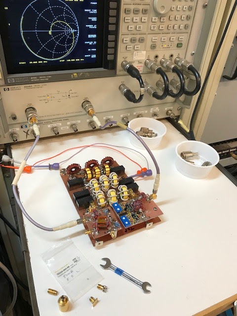
The Build:
Making the LPF board using scrap double-sided PCB stock. A Dremel tool plus engraving bit equals much work, but it gets the job done.
I tried to ensure that trace separation for the RF signals was at least 1/8th of an inch. I used the Microsemi PCB's trace separation as my model -- spacing on that board looks to be about 1.5 mm (i.e. 0.6"), so a goal of an 1/8th of an inch spacing is adding some margin.


Low-pass Filter, during VNA measurements:

The LPF Input Directional Coupler:

Note that the core for the current-sense transformer does not need to be as large as the voltage sense transformer (see here and here).
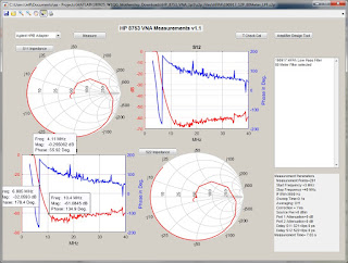
Filter Passband Measurements:
Filter S21 measurements were made with my HP 8753C Vector Network Analyzer. Its span was set wide enough to ensure that I would capture both the fundamental frequency as well as the 11th harmonic (should it be visible):

Here are the results for each filter:
80 Meter Filter:
40/30 Meter Filter:
Original Filter:
Note that the attenuation is only -12.5 dB at 14 MHz (the second harmonic of 7 MHz). This would become a problem when I measured actual PA Harmonic Distortion (measurement further below).

New Filter:
A simple change would be to add an additional turn to each of the filter's inductors to give me a bit more loss (7 dB) at 14 MHz without significantly affecting 30 meters.

20/17 Meter Filter:

15-10 Meter Filter:

Everything looks good on the VNA. Let's see how the actual PA Harmonic Distortion looks at 500 watts out...
Harmonic Distortion Measurements:
I measured harmonic distortion by driving the completed PA to 500 watts (as measured with the E4406A) with a CW tone and then measuring its output distortion with the same E4406A. Note the 50 dB attenuator between the Amplifier output and the E4406A input!

A laptop PC, using a MATLAB script (here) written by Dick Benson, W1QG, captures the spectrum data from the E4406A spectrum analyzer via GPIB. And note that the E4406A also has its internal attenuation set to 30 dB.
(Please see my notes, further below, for comments regarding the limitations of the E4406A).
Here are my measurements:
80 Meter Harmonic Distortion:

40 Meter Harmonic Distortion:
Original Filter:
Note that the level of the second harmonic is only 40.9 dB below the fundamental. FCC requires it be at least 43 dB lower.

Given that my VNA measurements showed filter-attenuation to be -12.5 dB at 14 MHz, this -40.9 dBc measurement implied that the second harmonic of 7 MHz prior to the LPF was at -28.4 dBc.
A possible fix might be to tweak the PA bias pots to improve symmetrical operation (because even-order harmonics are created when waveforms are non-symmetrical). And when I did this I got a dip in the second harmonic, but when I measured the bias currents for minimum second harmonic, Q1's Idd was 0.5 amps and Q2's Idd was 1.5 amps!
And Q2 was running significantly hotter, even while "idling" with bias on but no drive.
Not a good solution, in my opinion. So I adjusted the bias currents to be equal (at 0.5A each), and instead I lowered the cutoff frequency of the low-pass filter by adding a turn to each of the inductors.
New Filter:
With the redesigned filter, the second harmonic is now 49 dB lower than the fundamental:

What's weird is that, per the W6PQL website, his "Gen2" 40/30 meter filter should be down by 25 dB at 14 MHz (see https://www.w6pql.com/images/hf/gen2bp40-30.jpg). But I only saw 12.5 dB of attenuation -- that is a significant difference!
If I calculate the inductance values using "mini Ring Core Calculator" and then insert these values into ELSIE (along with the cap values -- note: using the values that sum to 510 pf, not the 521 pf stated in W6PQL's schematic), attenuation at 14 MHz is only -4.4 dB:

-4.4 dB is a very long way from the W6PQL website value of -25 dB. I can't explain this large difference. I would expect there to be some difference between calculated inductance versus actual "realized" inductance, but a variation that results in an additional 20 dB of attenuation would seem to be too much (although...it is a 7 pole filter and thus the slope is very steep!).
Anyway...my measured 12.5 dB of filter attenuation wasn't sufficient to bring the 14 MHz harmonic of 7 MHz into FCC compliance, so I looked for a simple way to modify the existing filter. I didn't need much additional attenuation.
After experimenting with ELSIE, I decided that adding a single turn to each of the three inductors was a reasonable way to go. Per ELSIE, attenuation at 14 MHz would increase by 8.2 dB. (Actual attenuation, per my measurements, above, show this increase to be 7.1 dB).
30 Meter Harmonic Distortion:

(Note, although I tested this at 500 watts into a dummy load, maximum power on 30 meters for Radio Amateurs in the U.S. is 200 watts, PEP).
20 Meter Harmonic Distortion:

17 Meter Harmonic Distortion:

15 Meter Harmonic Distortion:

12 Meter Harmonic Distortion:

10 Meter Harmonic Distortion:

With the redesigned 40/30 meter filter, everything now look copacetic!
Calculating Peak Capacitor and Inductor Voltages and Currents:
Making the LPF board using scrap double-sided PCB stock. A Dremel tool plus engraving bit equals much work, but it gets the job done.
I tried to ensure that trace separation for the RF signals was at least 1/8th of an inch. I used the Microsemi PCB's trace separation as my model -- spacing on that board looks to be about 1.5 mm (i.e. 0.6"), so a goal of an 1/8th of an inch spacing is adding some margin.


Low-pass Filter, during VNA measurements:

The LPF Input Directional Coupler:

Note that the core for the current-sense transformer does not need to be as large as the voltage sense transformer (see here and here).
Filter Passband Measurements:
Filter S21 measurements were made with my HP 8753C Vector Network Analyzer. Its span was set wide enough to ensure that I would capture both the fundamental frequency as well as the 11th harmonic (should it be visible):
Here are the results for each filter:
80 Meter Filter:

40/30 Meter Filter:
Original Filter:
Note that the attenuation is only -12.5 dB at 14 MHz (the second harmonic of 7 MHz). This would become a problem when I measured actual PA Harmonic Distortion (measurement further below).

New Filter:
A simple change would be to add an additional turn to each of the filter's inductors to give me a bit more loss (7 dB) at 14 MHz without significantly affecting 30 meters.

20/17 Meter Filter:

15-10 Meter Filter:

Everything looks good on the VNA. Let's see how the actual PA Harmonic Distortion looks at 500 watts out...
Harmonic Distortion Measurements:
I measured harmonic distortion by driving the completed PA to 500 watts (as measured with the E4406A) with a CW tone and then measuring its output distortion with the same E4406A. Note the 50 dB attenuator between the Amplifier output and the E4406A input!

A laptop PC, using a MATLAB script (here) written by Dick Benson, W1QG, captures the spectrum data from the E4406A spectrum analyzer via GPIB. And note that the E4406A also has its internal attenuation set to 30 dB.
(Please see my notes, further below, for comments regarding the limitations of the E4406A).
Here are my measurements:
80 Meter Harmonic Distortion:

40 Meter Harmonic Distortion:
Original Filter:
Note that the level of the second harmonic is only 40.9 dB below the fundamental. FCC requires it be at least 43 dB lower.

Given that my VNA measurements showed filter-attenuation to be -12.5 dB at 14 MHz, this -40.9 dBc measurement implied that the second harmonic of 7 MHz prior to the LPF was at -28.4 dBc.
A possible fix might be to tweak the PA bias pots to improve symmetrical operation (because even-order harmonics are created when waveforms are non-symmetrical). And when I did this I got a dip in the second harmonic, but when I measured the bias currents for minimum second harmonic, Q1's Idd was 0.5 amps and Q2's Idd was 1.5 amps!
And Q2 was running significantly hotter, even while "idling" with bias on but no drive.
Not a good solution, in my opinion. So I adjusted the bias currents to be equal (at 0.5A each), and instead I lowered the cutoff frequency of the low-pass filter by adding a turn to each of the inductors.
New Filter:
With the redesigned filter, the second harmonic is now 49 dB lower than the fundamental:

What's weird is that, per the W6PQL website, his "Gen2" 40/30 meter filter should be down by 25 dB at 14 MHz (see https://www.w6pql.com/images/hf/gen2bp40-30.jpg). But I only saw 12.5 dB of attenuation -- that is a significant difference!
If I calculate the inductance values using "mini Ring Core Calculator" and then insert these values into ELSIE (along with the cap values -- note: using the values that sum to 510 pf, not the 521 pf stated in W6PQL's schematic), attenuation at 14 MHz is only -4.4 dB:

-4.4 dB is a very long way from the W6PQL website value of -25 dB. I can't explain this large difference. I would expect there to be some difference between calculated inductance versus actual "realized" inductance, but a variation that results in an additional 20 dB of attenuation would seem to be too much (although...it is a 7 pole filter and thus the slope is very steep!).
Anyway...my measured 12.5 dB of filter attenuation wasn't sufficient to bring the 14 MHz harmonic of 7 MHz into FCC compliance, so I looked for a simple way to modify the existing filter. I didn't need much additional attenuation.
After experimenting with ELSIE, I decided that adding a single turn to each of the three inductors was a reasonable way to go. Per ELSIE, attenuation at 14 MHz would increase by 8.2 dB. (Actual attenuation, per my measurements, above, show this increase to be 7.1 dB).
30 Meter Harmonic Distortion:

(Note, although I tested this at 500 watts into a dummy load, maximum power on 30 meters for Radio Amateurs in the U.S. is 200 watts, PEP).
20 Meter Harmonic Distortion:

17 Meter Harmonic Distortion:

15 Meter Harmonic Distortion:

12 Meter Harmonic Distortion:

10 Meter Harmonic Distortion:

With the redesigned 40/30 meter filter, everything now look copacetic!
Calculating Peak Capacitor and Inductor Voltages and Currents:
I wrote a MATLAB routine to calculate peak capacitor and inductor voltages and
currents given 1) frequency of operation, 2) Component values and Q's, 3)
Voltage drive to the LPF (I assumed 600 watts driving power into 50 ohms to
calculate V), and 4) load SWR (I assumed 1.5:1 max SWR).
Given a target maximum load SWR, the MATLAB routine steps "around" the load's
constant-SWR circle (if envisioning a Smith chart) in one degree increments,
calculating the load's R+jX values at each step, and then the routine, given
this load value and the driving voltage, calculates the maximum voltage and
current for each component for that load.
The overall maximum voltage and current values (out of those calculated for
each of the 360 steps) for each component is noted, along with the angle at
which that max occurred.
To calculate power dissipation, component Q's can be assigned. I assumed
them to be 50 for the inductors and 1000 for the capacitors.
Power dissipation assumes long-term heating (rather than instantaneous power
dissipation). This amplifier is not designed to provide 600
watts continuous power. However, I would like to use it
as an amplifier for AM transmissions in which the modulated AM signal's peak
power is 600 watts (i.e. AM carrier power of 150 watts). Thus, for power
dissipation calculations, a carrier of 150 watts is the assumed output signal.
(Note that the calculator also allows me to add capacitors across the
inductors. I did not use such capacitors in this design, and thus they
are set to very small values (e.g. 0.1 pF) that have an insignificant effect
on the calculations).
Here are the MATLAB results:
80 Meter Filter:

40/30 Meter Filter:
At 7.15 MHz:

At 10.1 MHz:

20/17 Meter Filter:
At 14 MHz:


15/12/10 Meter Filter:
At 21.2 MHz:

At 24.9 MHz:

At 29.7 MHz:

1. I no longer recall why I have the calculations at the top of the form
for "At Maximum voltage across L3," but I'll note that this condition occurs
when the voltage across Zload is max. Given this condition, the
calculations show the SWR at the LPF's input, (given the 1.5:1 SWR
of the load), as well as the power dissipated by the load assuming the driving
signal is an AM carrier. Thus, given a driving voltage of 173.2 volts
peak (assuming SSB peak power of 600 watts into a 50 ohm load), the AM-carrier
drive voltage would be half this value, or 86.6 Vrms.
2. If you'd like to verify my results (or check my math for errors),
below are the important equations from the MATLAB routine. Note that 'k'
represents the angle of the load's Gamma that is being tested, and it steps
(in a loop) from 0 to 359 in steps of 1 (degree), ZL is the load impedance,
rho (the magnitude of Gamma) is calculated from the SWR (elsewhere), and Vin
is also calculated elsewhere.
Other Notes:
E4406A Limitations:
Dick Benson, W1QG, first informed me of the capabilities of the Agilent E4406A Vector Signal Analyzer "Transmitter Tester", and he has developed some MATLAB code for communicating with the tester via GPIB and analyzing its data (as seen, above).
From Dick's document describing his MATLAB code and the E4406A (found here)...
Some of the E4406A limitations are:
1) Its maximum "Span" is 10 MHz. This limits its utility as a general purpose Spectrum Analyzer.
2) Its first IF is 321.4 MHz, and the is no filtering before the first mixer. This means that images are very likely, and these can lead to confusion. For example, if the analyzer's center frequency is set to 50 MHz, the first LO will be set to 50+321.4 = 371.4 MHz. A signal fed into the analyzer at 692.8 MHz will produce an identical 321.4 MHz output from the first mixer since 692.8-371.4 = 321.4 MHz.
3) The input frequency range specs have a "hole": 7 to 314 MHz and 329 MHz to 4 GHz
4) There is no "Trace Memory" to allow A vs B measurement comparisons. Virtually all of these annoyances are addressed by the vsa_gui_1.m application.
Workarounds to the Limitations:
1) The 10 MHz maximum Span is addressed by stitching together multiple 10 MHz (or less) "chunks" of spectrum to cover a "Span" that is greater than the instrument's 10 MHz limit. This works remarkably well. But keep in mind that where the E4406a truly excels is in making narrow band measurements.
2) The mixer image problem can be addressed by using an external filter to limit the input signal frequency content to a known region. For instance, I use a 160 MHz low pass filter most of the time since my interests usually lie in the 3 to 160 MHz region.
3) It has been found that the analyzer works quite well down to about 1.5 MHz. Below this, the amplitude accuracy and linearity of the front end start to degrade. As to the hole between 314 and 329 MHz, well, just avoid it! However, you will find that most of this range is actually usable for narrow band analysis. Clearly an input signal at or very near 321.4 MHz should be avoided due to the first mixer RF-to-IF feed through.
4) Implementing "Trace Memory" is easy in MATLAB, and an invaluable feature.
And that's the end of this blog post. Continue on to the other posts in this series via the links, below...
K6JCA HF PA Posts:
Standard Caveat:
I might have made a mistake in my designs, schematics, equations, models, etc. If anything looks confusing or wrong to you, please feel free to leave a comment or send me an email.
Also, I will note:
This design and any associated information is distributed in the hope that it will be useful, but WITHOUT ANY WARRANTY; without an implied warranty of MERCHANTABILITY or FITNESS FOR A PARTICULAR PURPOSE.
radians = 2*pi*k/360;
gamma = rho*cos(radians) + rho*sin(radians)*1i;
ZL = Zo*(1+gamma)/(1-gamma);
RLD = real(ZL);
ZF1 = 1/(1/ZL1 + 1/ZC2);
ZF2 = 1/(1/ZL2 + 1/ZC4);
ZF3 = 1/(1/ZL3 + 1/ZC6);
Zout = 1/(1/ZC7 + 1/ZL);
ZB = 1/(1/ZC5 + 1/(ZF3 + Zout));
ZA = 1/(1/ZC3 + 1/(ZF2 + ZB));
Zin = 1/(1/ZC1 + 1/(ZF1 + ZA));
RIN = real(Zin);
VA = Vin * (ZA/(ZA + ZF1));
VL1 = Vin-VA;
VB = VA * (ZB/(ZB + ZF2));
VL2 = VA-VB;
Vout = VB*(Zout/(ZF3 + Zout));
VL3 = VB - Vout;
IC1 = Vin/ZC1;
IL1 = VL1/ZL1;
IC2 = VL1/ZC2;
IC3 = VA/ZC3;
IL2 = VL2/ZL2;
IC4 = VL2/ZC4;
IC5 = VB/ZC5;
IL3 = VL3/ZL3;
IC6 = VL3/ZC6;
IC7 = Vout/ZC7;
ILD = Vout/ZL;
IIN = Vin/Zin;
Keep in mind that the power dissipated by a component whose impedance
can be expressed as R+jX is simply the magnitude of the current through
the component, squared, times R.
Other Notes:
E4406A Limitations:
Dick Benson, W1QG, first informed me of the capabilities of the Agilent E4406A Vector Signal Analyzer "Transmitter Tester", and he has developed some MATLAB code for communicating with the tester via GPIB and analyzing its data (as seen, above).
From Dick's document describing his MATLAB code and the E4406A (found here)...
Some of the E4406A limitations are:
1) Its maximum "Span" is 10 MHz. This limits its utility as a general purpose Spectrum Analyzer.
2) Its first IF is 321.4 MHz, and the is no filtering before the first mixer. This means that images are very likely, and these can lead to confusion. For example, if the analyzer's center frequency is set to 50 MHz, the first LO will be set to 50+321.4 = 371.4 MHz. A signal fed into the analyzer at 692.8 MHz will produce an identical 321.4 MHz output from the first mixer since 692.8-371.4 = 321.4 MHz.
3) The input frequency range specs have a "hole": 7 to 314 MHz and 329 MHz to 4 GHz
4) There is no "Trace Memory" to allow A vs B measurement comparisons. Virtually all of these annoyances are addressed by the vsa_gui_1.m application.
Workarounds to the Limitations:
1) The 10 MHz maximum Span is addressed by stitching together multiple 10 MHz (or less) "chunks" of spectrum to cover a "Span" that is greater than the instrument's 10 MHz limit. This works remarkably well. But keep in mind that where the E4406a truly excels is in making narrow band measurements.
2) The mixer image problem can be addressed by using an external filter to limit the input signal frequency content to a known region. For instance, I use a 160 MHz low pass filter most of the time since my interests usually lie in the 3 to 160 MHz region.
3) It has been found that the analyzer works quite well down to about 1.5 MHz. Below this, the amplitude accuracy and linearity of the front end start to degrade. As to the hole between 314 and 329 MHz, well, just avoid it! However, you will find that most of this range is actually usable for narrow band analysis. Clearly an input signal at or very near 321.4 MHz should be avoided due to the first mixer RF-to-IF feed through.
4) Implementing "Trace Memory" is easy in MATLAB, and an invaluable feature.
And that's the end of this blog post. Continue on to the other posts in this series via the links, below...
K6JCA HF PA Posts:
- A 500 Watt HF PA, Part 1: Overview
- A 500 Watt HF PA, Part 2: PA (and Bias) Assembly
- A 500 Watt HF PA, Part 3: Low-pass Filter Assembly (including LPF-Input Directional Coupler)
- A 500 Watt HF PA, Part 4: Power Supply and Supervisory Circuitry
- A 500 Watt HF PA, Part 5: T/R Switching and Output Directional Coupler
- A 500 Watt HF PA, Part 6: Front Panel and Controller Assembly
- A 500 Watt HF PA, Part 7: Back Panel, Interconnects, and Miscellaneous
- A 500 Watt HF PA, Part 8: Complete Schematics
Standard Caveat:
I might have made a mistake in my designs, schematics, equations, models, etc. If anything looks confusing or wrong to you, please feel free to leave a comment or send me an email.
Also, I will note:
This design and any associated information is distributed in the hope that it will be useful, but WITHOUT ANY WARRANTY; without an implied warranty of MERCHANTABILITY or FITNESS FOR A PARTICULAR PURPOSE.


1 comment:
Nice Post.
Post a Comment