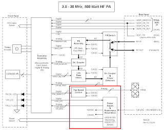
This blog post will describe the amplifier's Power Supply and Power Supply Supervisory circuitry. It also includes the Fan Speed control circuit.
These circuits are outlined in red in the block diagram, below:
Power Supply Circuitry:
Power Supply Schematic:
1. Each of the Meanwell switching power supplies has been adjusted to its maximum output voltage (about 31 volts for this particular power supply).
2. Diodes D1 and D2 were added per Meanwell's recommendation when connecting their supplies in series. Diode Vprv was selected per Meanwell's recommendation that it be "V1 + V2". I.e. at least 62 volts.
3. A DC-DC converter module is installed on the Controller board to provide 12V for the Amplifier's circuitry. This module uses an LM2596 voltage regulator whose input is rated to 40V maximum "operating" voltage. So I use the "lower" of the two Meanwell switching supplies (that is, the one whose negative output is grounded) to provide 31 volts to this module's input.
4. The connectors J2/J3 are not keyed, so it's possible to apply a negative voltage to the LM2596 module. I added diode D5 to prevent damage to the module should this occur. But, given that reversing J3 would also short out the lower switching power supply to ground, there might be larger problems if I were to do this. (I really should look around for a keyed connector and replace J2 and J3.)
5. The Input AC Voltage specifications of the Meanwell RSP-750 switching power supplies is 90 to 264 VAC, which meets my goal of 120 VAC input, but it also means that I could run this PA from 240 VAC without any changes (except for the value of the fuse on the back panel).
LM2596 Module Schematic:
I purchased 10 of these boards via eBay at a great price, only to discover that the price was great because the LM2596 Voltage Regulator chips were counterfeit.
So, per one of the notes in the schematic, below, remove the counterfeit and stuff the board with a real LM2596!
Other notes:
1. I also replaced the potentiometer with a fixed resistor. After all, pots can fail. And I don't need the output voltage to be adjustable for this application. It just needs to be approximately 12V (in this case, it's about 12.5 volts).
Power Supply Supervisory Circuit Schematic:
The Supervisory circuit monitors Vdd, Idd, and provides a means to quickly shut off Vdd to the PA should a fault condition occur.
Notes on the Supervisory Circuit Schematic:
1. Vdd shutoff is handled with an SUP7010El P-Channel FET, rated at 100V. Its RDS(on) is spec'd at about 10 milliohms for Vgs of -10V. So, if Idd were 20 amps, the voltage drop across this device would be only 0.2 volts and the dissipated power about 4 watts.
2. When the conrol signal VDD_OFF is driven high (i.e. when a Fault is detected), Q3 turns on, turning on Q4 which in turn forces Q1's Vgs to 0, turning Q1 off. C23 speeds up the turn-on time of Q4, ensuring the Idd shuts off more quickly.
3. Vdd is monitored with the voltage divider formed by R10 and R11.
4. An ACS722-20 monitors current (similar to the circuit in the Elecraft KPA-500). Note that the ACS722-20 has a maximum spec'd current of 20 amps, although I've found I can take mine about 10% higher. But, in my opinion, it is always a BAD IDEA to count on a component operating properly beyond its specifications, and so I've added a small amount of shunt resistance across the ACS722 so that I can monitor Idd currents slightly higher than 20 Amps but still remain within the ACS722-20's spec.
5. R12/C17 is a simple one-pole low-pass filter to suppress any unwanted RF that might be induced upon the cabling by the PA's RF fields. Ditto for R9/C6, as well as C16.
6. Note that J5 is a dual in-line header. This allows me to route ground (i.e. signal return) next to every signal in the cable. Doing so minimizes the "loop area" of each signal and its return, and thus minimizes induced interference from external B-fields.
(I always try to route a signal's return next to the signal itself -- by reducing the complete path's loop-area, not only do I minimize radiated interference from the signal (if it were a digital signal), but this technique also reduces a signal's susceptibility to external interference. And it's a much less expensive technique than using ferrites!)
Fan Speed Control Schematic:
Notes on the Fan Speed Control Schematic:
1. I've adapted (with some changes) the Fan Speed circuit from the Elecraft KPA-500.
2. D1 provides a discharge path for C5 (refer to TI's LM317HV datasheet). Normally, the fans should provide an adequate discharge path so that D1 would probably not be needed, but...if the cable connecting the fans to this circuit ever worked itself loose (or if I forgot to plug it in), then the diode would be very welcome, indeed!
3. The R-C combos of R5/C8, R12/C7, and R7/C9 are simple 1-pole filters to suppress any unwanted signals that might have been induced upon the control lines by external RF fields (of which there are plenty in a PA!).
4. Note that, for some reason, there seems to be a version of the 2N7002 transistor in my Orcad library that look like a bipolar device. Q1, Q3, and Q9 are not bipolar, they are FETs.
The Build:
Power Supplies:
(Not much to show!)
And that's the end of this blog post. Continue on to the other posts in this series via the links, below...
K6JCA HF PA Posts:
- A 500 Watt HF PA, Part 1: Overview
- A 500 Watt HF PA, Part 2: PA (and Bias) Assembly
- A 500 Watt HF PA, Part 3: Low-pass Filter Assembly (including LPF-Input Directional Coupler)
- A 500 Watt HF PA, Part 4: Power Supply and Supervisory Circuitry
- A 500 Watt HF PA, Part 5: T/R Switching and Output Directional Coupler
- A 500 Watt HF PA, Part 6: Front Panel and Controller Assembly
- A 500 Watt HF PA, Part 7: Back Panel, Interconnects, and Miscellaneous
- A 500 Watt HF PA, Part 8: Complete Schematics
Standard Caveat:
I might have made a mistake in my designs, schematics, equations, models, etc. If anything looks confusing or wrong to you, please feel free to leave a comment or send me an email.
Also, I will note:
This design and any associated information is distributed in the hope that it will be useful, but WITHOUT ANY WARRANTY; without an implied warranty of MERCHANTABILITY or FITNESS FOR A PARTICULAR PURPOSE.


No comments:
Post a Comment