
This post will describe the Amplifier's T/R Switching circuitry and its Output Directional Coupler circuitry:

T/R Switch and Directional Coupler Schematic:

Notes on the T/R Switch and Directional Coupler Schematic.
1. My FGPA-SDR transceiver doesn't use QSK. Therefore, no QSK!
2. The Directional Coupler at the output of the T/R switch allows me to monitor power going to the antenna even when I'm not using the PA (but the PA does need to be turned on).
3. I've described designing and building Directional Couplers in a number of blog posts. See here, here, and here, for example. This directional coupler is just another one in the series.
4. Note that the Directional Coupler's calculated coupling factor is 28 dB (based upon the number of windings on each transformer). Therefore, if I'm transmitting in the range of 500 to 600 watts out, the Directional Coupler's FWD signal will be nearly a watt! (i.e. about 29 dBm).
5. Note that the signals on J15 have their signal returns (in this case, ground) on adjacent pins, for mitigating EMI susceptibility.
(I always try to route a signal's return next to the signal itself -- by reducing the complete path's loop-area, not only do I minimize radiated interference from the signal (if it were a digital signal), but this technique also reduces the signal's susceptibility to external interference. And it's a much less expensive technique than using ferrites!)
Attenuators Schematic:

Notes on the Attenuators Schematic:
1. The termination at the FWD port should be able to dissipate 1 watt (see explanation, above).
2. Assuming the PA's load has an SWR of 2:1 or better, then, for 500 watts out, the reflected power will be, at most, about 56 watts. This value is reduced by the Directional Coupler's Coupling Factor of 28 dB. Thus, the power at the REF port should 56 watts attenuated by 28 dB, or about 0.1 watts.
3. The power at the FWD connector is split into two paths of equal attenuation (22 dB each). One path will continue on to the FWD power detector (see next schematic), and the other path goes to an SMA connector on the PA's front panel for monitoring the RF Output signal with, for example, either an oscilloscope or a spectrum analyzer.
4. The total attenuation for both FWD and REF power paths (including the directional coupler's coupling factor) is 50 dB.
5. If the RF Sample port were terminated in 50 ohms, and if all resistor values actually equaled those in the schematic, and if the load at the VOUT_FWD port were 50 ohms, then the input impedance at the FWD port (on the left side of the page) would be 49.93 ohms (i.e. Return Loss of 62.6 dB).
Forgetting to terminate the RF sample port would change the FWD port's input impedance from 49.93 ohms to 50.44 ohms (i.e. Return Loss of 47.3 dB). Still pretty good. But the voltage at VOUT_FWD would increase by about 20% (according to LTSpice), erroneously increasing the Forward Power reading.
Power Detectors Schematic:
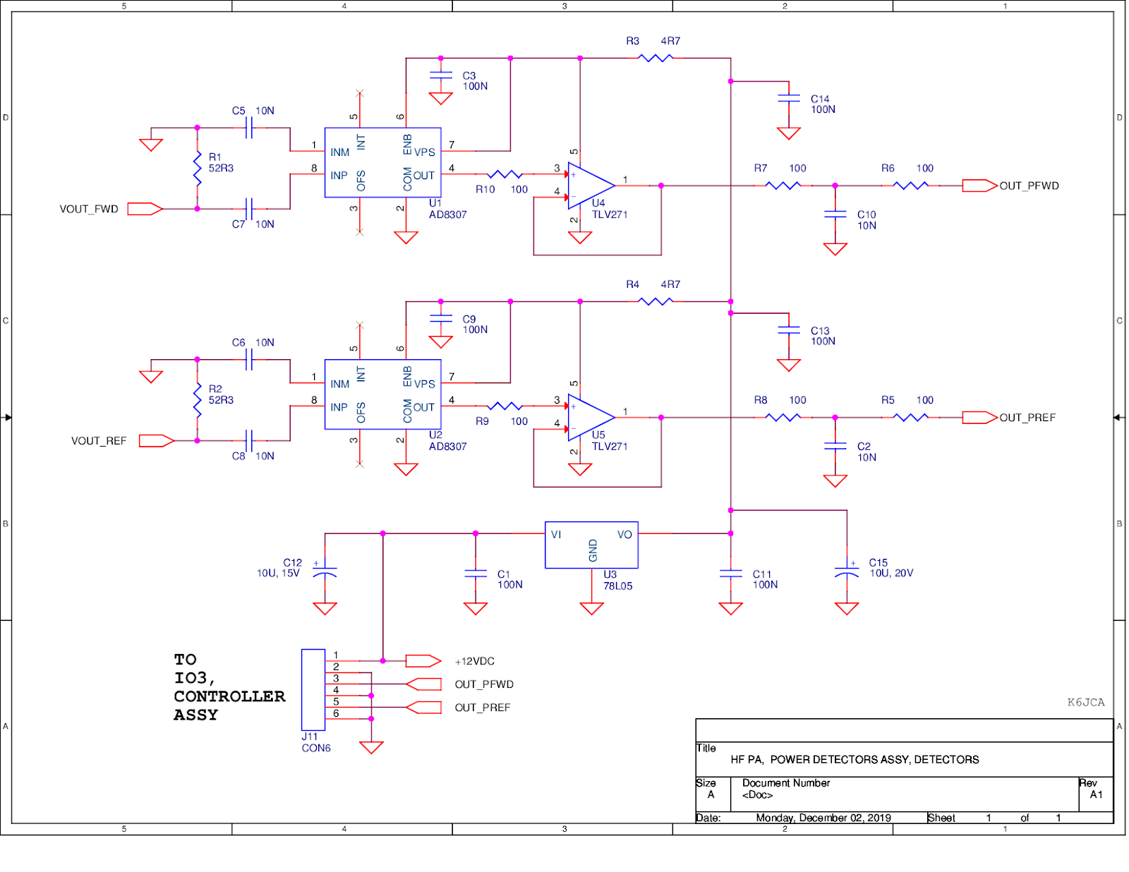
Notes on the Power Detectors Schematic:
1. I use AD8307 log detectors to convert the FWD and REF power to a dB level. Note that these detectors can handle a maximum input of only +17 dBm, thus I've attenuated their inputs by 50 dB (as described, above). In other words, a 500-watt Forward-power signal (+57 dBm) should be down to +7 dBm at the AD8307.
2. The AD8307 devices are wired per the "Basic Connections" figure in their datasheet (figure 32).
3. Each AD8307 output is buffered with a unity-gain, rail-to-rail op-amp (TLV271). This op-amp isolates the AD8307's output (which looks like 12.5K ohms to ground) from the unwanted influence of any downstream loads.
4. The output of each op-amp connects to an R-C-R "T" network: R7/C10/R6 and R8/C2/R5.
The R6/C10 and R5/C2 R-C pairs form simple 1-pole filters to suppress any RF that might be induced onto the cables (from external RF fields) from reaching the outputs of the two op-amps.
Resistors R7 and R8 help isolate the op-amps' outputs from the capacitive-loading effects of C10 and C2.
5. Resistors R9 and R10 are not needed. I had installed them before I realized that I needed to add the op-amp buffers (because of loading on the AD8307 output resistor), and I was too lazy to remove them.
6. Note that the signals on connector J11 have their signal-returns on adjacent pins (to minimize overall path loop-area and thus reduce susceptibility to RF fields).
The Build:
Unfortunately, I don't have any pictures of these assemblies outside of the PA. Never the less, here are a few photos...
The back of the T/R assembly. These are the pads for the relays:

The construction of the Directional Coupler part of this assembly follows the spirit of this wiring diagram (from here), but the current-sense transformer is smaller, as is the overall volume of space used.

You can get an idea of how it actually looks with these two photos...
First, the voltage-sense transformer:

(the two black shapes to the left are the T/R relays).
And the current-sense transformer :

Finally, here's a photo of the Attenuator and Power Detector assembly:

Directional Coupler Measurements:
The Directional Coupler is a 4-port device. Let's assign the following Port numbers to the Directional Coupler's ports:
1 = Input Port
2 = Output Port
3 = FWD Port
4 = REF Port
I will use these port numbers to reference the appropriate S-parameter measured with my HP 8753C VNA. Note that all of the measurements below (with the exception of S12) use the VNA's S21 results. I then interpret the S21 results to be S31, S32, etc., depending upon how I had connected the VNA's two ports to the Directional Coupler's ports.
Driving Port 1 (the IN port):
Measuring S21 and S12:
VNA Port 1 = Directional Coupler "IN" Port.
VNA Port 2 = Directional Coupler "OUT" Port.
Directional Coupler "FWD" Port terminated in 50 ohms.
Directional Coupler "REF" Port terminated in 50 ohms.

Measuring S31:
VNA Port 1 = Directional Coupler "IN" Port.
VNA Port 2 = Directional Coupler "FWD" Port.
Directional Coupler "OUT" Port terminated in 50 ohms.
Directional Coupler "REF" Port terminated in 50 ohms.

Measuring S31 (with OUT port OPEN):
VNA Port 1 = Directional Coupler "IN" Port.
VNA Port 2 = Directional Coupler "FWD" Port.
Directional Coupler "OUT" Port OPEN.
Directional Coupler "REF" Port terminated in 50 ohms.

Measuring S41:
VNA Port 1 = Directional Coupler "IN" Port.
VNA Port 2 = Directional Coupler "REF" Port.
Directional Coupler "OUT" Port terminated in 50 ohms.
Directional Coupler "FWD" Port terminated in 50 ohms.

Measuring S41 (with OUT port OPEN):
VNA Port 1 = Directional Coupler "IN" Port.
VNA Port 2 = Directional Coupler "REF" Port.
Directional Coupler "OUT" Port OPEN.
Directional Coupler "FWD" Port terminated in 50 ohms.

Driving Port 2 (the OUT port):
Measuring S42:
VNA Port 1 = Directional Coupler "OUT" Port.
VNA Port 2 = Directional Coupler "REF" Port.
Directional Coupler "IN" Port terminated in 50 ohms.
Directional Coupler "FWD" Port terminated in 50 ohms.

Measuring S42 (with IN port OPEN):
VNA Port 1 = Directional Coupler "OUT" Port.
VNA Port 2 = Directional Coupler "REF" Port.
Directional Coupler "IN" Port OPEN.
Directional Coupler "FWD" Port terminated in 50 ohms.

Measuring S32:
VNA Port 1 = Directional Coupler "OUT" Port.
VNA Port 2 = Directional Coupler "FWD" Port.
Directional Coupler "IN" Port terminated in 50 ohms.
Directional Coupler "REF" Port terminated in 50 ohms.

Measuring S32 (with IN port OPEN):
VNA Port 1 = Directional Coupler "OUT" Port.
VNA Port 2 = Directional Coupler "FWD" Port.
Directional Coupler "IN" Port OPEN.
Directional Coupler "REF" Port terminated in 50 ohms.

Calculating the Directional Coupler's parameters:
Directivity is an important parameter, and it can be calculated for both the REF port and the FWD port of the Directional Coupler.
Per this reference, Directivity of the FWD port is: S31(dB) + S21(dB) - S32(dB)

We can calculate the Directivity of the REF port in a similar fashion: S42(dB) + S12(dB) - S41(dB).
Here's a MATLAB plot of the REF port Directivity (using the data captured with my 8753C and displayed earlier in this blog post):

The red curve gets pretty noisy because the measurement is approaching the noise floor of the VNA. Thus, Directivity looks noisy, too, which is the reason why I added the "Smoothed Directivity" curve (smoothed with a 31 point moving-average filter -- which is why it doesn't track too well at the far right-hand side: the filter is running out of data).
And here's a plot of FWD port Directivity:

Therefore the Directional Coupler's Parameters (at 29.91 MHz) are:

Note that the important directivity value is the REF port's directivity. If it's poor, then forward-power undesirably coupled into this port could significantly affect the actual reflected power reading, if SWR is low.
Conversely, the quality of the FWD port's directivity isn't as important, because if the load is fairly well matched, reflected power should already be fairly low compared to forward power, and the likelihood of reflected power leakage into the FWD port (due to poor directivity) significantly affecting the FWD power measurement is therefore lessened.
Fortunately, at 53.7 dB, the REF port's directivity is excellent.
And the FWD port's directivity of 30 dB is pretty good, too.
A Simpler Method to Determine REF Port Directivity:
The above calculations go by the book, using the exact definition of Directivity, in which both the Input port and the Output port of the Directional Coupler are driven.
But you can determine Directivity of the REF port fairly easily without having to drive the Output port (i.e. without having to measure S42).
You still need two measurements, but you can make them by driving only the Directional Coupler's Input port.
First, drive the Input port, with the Output port terminated in 50 ohms, and measure the power at the REF port.
Then remove the 50 ohm termination from the Output port (i.e. the Output port is now OPEN) and, again driving the Input port, remeasure power at the REF port..
To calculate Directivity, simply subtract the first measurement from the second measurement.
(If you leave the Output port open while driving the Input port, then all of the Output power is reflected back, and this mimics driving the Output port.)
Of course, this method assumes negligible insertion loss.
If you look at my S21 captures earlier in this post you'll see that I captured S41 with the output terminated and S41 with the output open (that is, I drove the Input port and measured REF power with the Output port terminated and then open). Let's use that data to calculate the REF's port Directivity:
Here are the results:

How close are these results to the earlier "by-the-book" results? Let's compare the two by subtracting one from the other...

Less than 0.1 dB difference. Pretty darn close!
And that's the end of this blog post. Continue on to the other posts in this series via the links, below...
K6JCA HF PA Posts:
- A 500 Watt HF PA, Part 1: Overview
- A 500 Watt HF PA, Part 2: PA (and Bias) Assembly
- A 500 Watt HF PA, Part 3: Low-pass Filter Assembly (including LPF-Input Directional Coupler)
- A 500 Watt HF PA, Part 4: Power Supply and Supervisory Circuitry
- A 500 Watt HF PA, Part 5: T/R Switching and Output Directional Coupler
- A 500 Watt HF PA, Part 6: Front Panel and Controller Assembly
- A 500 Watt HF PA, Part 7: Back Panel, Interconnects, and Miscellaneous
- A 500 Watt HF PA, Part 8: Complete Schematics
Standard Caveat:
I might have made a mistake in my designs, schematics, equations, models, etc. If anything looks confusing or wrong to you, please feel free to leave a comment or send me an email.
Also, I will note:
This design and any associated information is distributed in the hope that it will be useful, but WITHOUT ANY WARRANTY; without an implied warranty of MERCHANTABILITY or FITNESS FOR A PARTICULAR PUR


No comments:
Post a Comment