(Part 3 of this series is here: Part 3)
But before I begin, let me again acknowledge Dick Benson, W1QG. Dick is the father of this design, and although I've made some modifications to the FPGA logic, the underlying architecture and the vast majority of the Simulink implementation is Dick's.
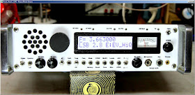
In the last image, above, the box at the left side of the chassis contains the receiver's Broadcast-Band Reject filter, the Anti-Aliasing filter, and the RF preamp(s). The PIC controller is on the board that spans the chassis from left-to-right, just behind the front panel at the bottom of the image. And the FPGA board with ADC, DAC, and Audio Codec (and miscellaneous circuitry) is the copper-clad board taking up the majority of the chassis area.
Please note that Dick's transmitter's PA (and an Antenna Tuner) are in a separate box. The PA amplifies the transceiver's 10 dBm output (10 milliwatts) up to 100 watts, and is based upon Motorola's app notes AN-762 and AN-779. The tuner is of Dick's own design:
Audio and Mode Control:
Let's return to the Simulink Xilinx model for the radio. In this blog post I will focus on the Audio and Mode Control subsystem, highlighted below with the yellow circle.
(Click on image to enlarge)
If we open this block, we see blocks for audio processing (the "Audio_Processor" and the "AGC_and_More" blocks), and blocks for control ("Reg_A," "Reg_B," and "T_R_Delay"). Let's first look at these control blocks, which I've highlighted, below:
(Click on image to enlarge)
Audio Control:
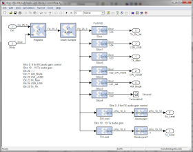
Registers A and B are 26-bit wide write-only registers to control some of the transceiver's functions. Their subsystem models are shown below and should be self-explanatory.
(Click on image to enlarge)
The T_R_Delay subsystem is shown below.
(Click on image to enlarge)
Notes on the T_R_Delay subsystem:
- This subsystem runs at the Audio sample rate of 9,765.625 KHz (period = 0.1024 ms).
- The Tx/Rx output mimics the input Tx_Rx_bit, but it is delayed by 70 clocks (about 7.2 ms) to compensate for the clearing of the Information Filter when going from Rx to Tx (This clearing takes about 13 ms, so about 6 ms will be clipped from the leading edge of the first CW character. Without this delay 13 ms would be clipped, instead.)
- The Tx_Rx_Delayed output goes high when the Tx_Rx_bit input goes high (i.e. upon entering Tx mode), but, after Tx_Rx_bit goes low, it holds its high state for a length of time determined by its Delay input (Hold Time = Delay * 0.1024 ms). This signal is meant to be used for controlling, for example, the antenna relay.
- The Tx_Rx_D40 output is simply Tx_Rx_Delayed with its leading (high-going) edge delayed by 40 clocks. This allows the RX EQ filter (whose depth is 64 samples) to (mostly) clear out before being used for sidetone. Otherwise, an audio artifact can be heard on the first CW leading edge when Tx_Rx_Delayed goes high.
- Ideally, Tx/Rx, when high, should be bracketed within Tx_Rx_Delayed, so that, for example, the antenna relay switches to the transmitter before actual RF is generated, and switches back to the receiver after transmission has ended. Therefore, if Tx/Rx has a delay of 7 ms, then Delay should be set to be at least 7 ms (i.e. at least a count of 70).
Now let's look at the Receive Audio path...
Receive Audio Path:
Let's return to the Audio_and_Mode_Control subsystem:
(Click on image to enlarge)
Receive audio comes into this subsystem from the demodulator, passes through the "AGC_and_More" subsystem, and then is serialized and sent to the external Audio Codec.
I've highlighted this receive audio path, below:
(Click on image to enlarge)
Let's open up the AGC_and_More subsystem and see what is going on inside it.
AGC_and_More Subsystem:
This subsystem contains the AGC circuitry (used for both Tx and Rx gain control), an Rx Audio Filter (which I might from time to time also call the RX EQ filter), a multiplier block, "Time_Share_MPY" for controlling receive volume and Tx power, and various blocks for audio sources and destinations.
(Click on image to enlarge)
Let's first look more closely at the "AGC Xilinx" block, which I've highlighted, below:
(Click on image to enlarge)
AGC_and_More -- AGC Xilinx Subsystem:
The "AGC Xilinx" block contains the AGC subsystem. This AGC subsystem is used both for Tx (to bring up mic audio) and for Rx.
As Dick, W1QG points out:
The "traditional" analog radio AGC has always (to my knowledge) been a feedBACK scheme.
The analog RX has lots of gain before the detector and this gain is reduced as a function of the signal strength.
The sensing of signal strength can occur before, after, or in the detector stage.
This radio uses a feedFORWARD scheme where the gain before the detector is fixed, and in fact, limited to essentially 1 (selectable 0,6,12,18dB gains at the CIC Filter output not withstanding).
The signal after the detector is increased as a function of the inverse of signal strength.
(Click on image to enlarge)
But before getting into the details of the AGC functions, let's first take a quick look at the control register, "AGC_Reg", in the lower left-hand corner.
AGC_and_More -- AGC Xilinx -- AGC_Reg:
(Click on image to enlarge)
This register's function should be fairly obvious, but I do want to point out the multiplexer at the top. This circuit ensures that the Max_Rx_Gain field can never be set (by software) to zero. If it were to be zero, then there is the possibility that the AGC's divider could divide by zero. This circuit prevents that possibility from occurring.
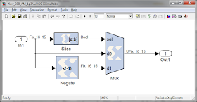
Now let's look at some of the subsystems within the "AGC Xilinx" block. The first is "Xabs", and its output is the absolute value of its input.
Now let's look at some of the subsystems within the "AGC Xilinx" block. The first is "Xabs", and its output is the absolute value of its input.
AGC_and_More -- AGC Xilinx -- Xabs Subsystem:
The next subsystem within the AGC Xilinx block is the "Attack Filter" subsystem.
AGC_and_More -- AGC Xilinx -- Attack Filter Subsystem:
The "Attack Filter" subsystem is simply a one-pole low-pass IIR filter that has two different attack values. Dick's 15/16 coefficient equates to an attack time of 1.6 ms, but I found that this attack time was too slow in high QRN environments -- it did not track the peaks of the QRN noise and I would hear the QRN pulses, after AGC attempted to limit them, banging up against the full-scale values of the data path (+/- 1).
So I fixed this problem by adding an optional attack time of 0 ms -- in other words, the second low-pass filter option for attack-time is...no low pass filter. This option has the benefit of ensuring that AGC'ed audio, be it Tx or Rx audio, never can be driven hard enough to "saturate" at the data path's maximum limits. And its drawback is that random noise spikes can cause the AGC to artificially depress receive audio, and it can take some time to recover if the AGC decay rate is set to be a long period.
But so far this drawback has not been much of an issue, whereas, for me, the benefit of zero-attack is obvious. (and if it does become an issue, I have some thoughts as to how it might be mitigated).
Notes on the values of CMult1 and CMult3...
Before I discuss CMult1 and CMult3, I should explain that the goal of the AGC is to amplify an audio sample (whose value, in the case of receiver audio, will be typically very small) up to, but not to exceed, +/-1 -- the Full Scale limits of the signals.
This amplification is done by a division process in which the received sample is divided by a number, in this design called the divisor (for obvious reasons). If this divisor equals the received sample's absolute value, the output will be 1 (or -1, if the sample is negative). And in which case we have just snugged up to, but not exceeded, our limits.
And if the divisor is larger than the sample's absolute value, then the result will be less than +/- 1, which is OK, too, depending upon our goals.
But if the divisor is smaller than the sample's absolute value, we will have problems, because then the result will exceed +/- 1 and the signal will be clipped, resulting in distortion.
So one main goal of the AGC is to try to ensure that the divisor is never smaller than the absolute value of the sample it is being divided into.
My AGC circuit simplifies this process, because I simply pass the absolute value of the received sample along as the divisor. So the sample will, worst case, be divided by itself and the result can never exceed +/- 1, in theory.
But that's in theory. Because I'm always a bit worried about errors within fixed point arithmetic and other unknown unknowns, I thought it better to limit the divider's maximum output to be slightly less than +/- 1, which is why the divisor's gain, set by CMult3, is 1.1875 (1 + 3/16), rather than being equal to 1. So the maximum range of the divider's output should be at most +/- 0.84, rather than +/- 1.0. In other words, about 1.5 dB below Full Scale.
Dick's CMult1 also has a gain factor. If there were no gain, the value of his b0 coefficient should be 1/16 (that is, equal to 1 - 15/16, or 0.0625). But b0 is actually 0.1875 -- three times the value of 1/16.
In other words, Dick has essentially followed his attack filter with a gain-stage of 3.
In large part, I believe this additional gain is to compensate for the delayed (low-pass filtered) response of the attack filter and its inability to track fast-attack signals (e.g. noise), thus allowing them to drive into saturation unless compensated with additional divisor gain, in this case, 3.
(For more on single pole IIR filters, please see the section, Single-Pole Low-Pass IIR Digital Filter notes..., at the end of this blog post.)
AGC_and_More -- AGC Xilinx -- Leaky Peak Detector Subsystem:
The Attack Filter then feeds into a Leaky Peak Detector, shown below:
(Click on image to enlarge)
The Leaky Peak Detector's goal is to detect signal peaks from the Attack Filter and then to hold these peaks, using their values to set the AGC gain.
But we do not want the peak detector to be a perfect detector -- we want the level to slowly decay so that, as band conditions change (e.g. QSB) or signals change, the AGC circuit will adjust to new, perhaps lower, signal peaks.
Currently, the Leaky Peak Detector has four rates of decay:
- Slow: 840 ms.
- Fast: 210 ms.
- Very Fast: 26 ms.
- Ultra Fast: 6.5 ms.
Note that the Peak Detector is designed to maintain the last peak value of the receive audio during transmit, and the last peak value of the transmit audio during receive.
AGC_and_More -- AGC Xilinx -- Hang Time Subsystem:
The AGC circuit also includes a Hang Time provision:
(Click on image to enlarge)
If a new peak is detected by the Leaky Peak Detector, rather than have the Leaky Peak Detector immediately begin to leak, the peak value can be held for some amount of time (the Hang Time), and then, after the Hang Time period has elapsed, allowed to decay.
Other Hang Time notes:
- Hang time can be set to be between 0 and 1.6 seconds, adjustable in 52.4 ms increments.
- Currently, a single value of Hang Time is stored in the hardware, and if a user desires it to be different for Tx versus Rx, it must be loaded by the Host (i.e. UI) Processor (Arduino in my case, PIC in Dick's) with the appropriate value when transitioning between Tx and Rx.
- The Hang Time counter is automatically reset when transitioning between Rx and Tx states.
AGC_and_More -- AGC Xilinx -- Sample Delay Subsystem:
There is delay through the AGC divisor's path (consisting of the attack filter and the leaky-peak detector), and the Sample Delay subsystem attempts to apply a corresponding delay to the dividend's path so that the dividend (the audio sample to be amplified) arrives at the divider with an appropriate divisor.
(Click on image to enlarge)
In the case of my version of the AGC (no attack filter), this is straightforward -- the divisor has a delay of 2 clocks through the attack and leaky-peak detector, and so I delay the audio-sample-to-be-divided by the same amount: 2 clocks.
Compensation is a bit more complicated for Dick's AGC with the 16 sample time constant. He adds a delay of 18 clocks, but is this enough? For example, given a step-function input, it is quite possible that the divisor has not risen to its full value, given the 16-sample time constant, after 18 clocks (although this will depend in some part upon the step-function's rise time, itself, when it arrives at the AGC block as audio -- the leading edge will have some slope and not be a zero rise-time).
So, if the Divisor is smaller than the Dividend when they both arrive at the AGC divider, there is the very real possibility of driving the signal into the rails. And this is probably one of the reasons why Dick has a gain of 3 after his Attack Filter.
AGC_and_More -- AGC Xilinx -- Sequential Divide Subsystem:
And now we come to the AGC divider circuit!
Within the block above is a circuit which limits the maximum gain that can be applied to a signal. Let's look at it, first.
(Click on image to enlarge)
This circuit allows the user to limit the amount of gain that AGC can apply, and it does this by limiting how small the Divisor can become (the smaller the divisor is, the more gain the AGC applies). This level is set by the user via the Max_RX_Gain word.
So if the divisor value entering this block is less than Max_RX_Gain, this circuit forces the divisor value to be limited to Max_RX_Gain, thus limiting the maximum gain in RX mode.
Note that in the AGC_Reg subsystem there is a circuit which forces the Max_RX_Gain value to be at least 1. I added this to prevent the Divisor from having an unintentional "Divide-by-zero" situation.
But this circuit is not strictly needed -- the Host Processor's software, which must load this value, could guarantee that it is never zero. And I'm not convinced that there is a divide-by-zero issue with Dick's "Sequential Divide" circuit (to be discussed in just a paragraph or two).
(I will also point out that there is an adder circuit after this limiter, but a value of 0 is added, so it has no effect. Dick's AGC circuitry doesn't have the same limiter, but he does have this adder which he uses to add a value of 2^-16 to the Divisor -- that is, he adds 0x0001 to the Divisor).
Let's take a quick look at the theory behind the AGC Divider...
Sequential Divide Theory:
As Dick mentioned earlier in this post, the AGC system is a FeedForward system in which the "signal after the detector is increased as a function of the inverse of signal strength."
This increase is performed by a division function, where the signal (the Dividend) is divided by a Divisor to create an amplified signal. The lower the signal strength, the smaller will be the value of the Divisor. If the Dividend and Divisor are equal in amplitude, we want the output to be +1 (the maximum for a positive signal) or -1 (for a negative signal). Both of these values represent the AGC output after maximum amplification is applied to the Dividend, prior to clipping distortion (and actually, +1 is clipping by just a hair's width).
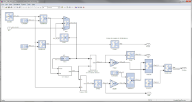
Below is the Simulink model of the Divider circuit. But note, there's a multiplier in the heart of it!
(Click on image to enlarge)
You are probably thinking, "but isn't calculating 1/x just as difficult as dividing?"
Dick takes a clever approach to this calculation, recognizing that we do not need a precise number for 1/x -- after all, this is an AGC circuit and we just need to ensure that the output value from the AGC circuit is close to one if the Dividend and the Divisor are equal. The result does not need to always be exactly 1.
So, why not find 1/x with a simple ROM lookup table?
So, being a binary system with the Divisor's data format being an Unsigned 16 bit word whose decimal point is at bit 16 (i.e. the maximum value of this word is ever so slightly less than +1.0), Dick does the following:
1. Shift the Divisor left until the MSB of the shifted divisor is 1. (And remember the amount the Divisor had to be shifted -- this number will be used, later)
2. Recognizing that the value of the shifted divisor now lies between 0.5 and 0.999... (note that, with the MSB set, the value represented at the low end by 0x8000 is 0.5 and and at the high end by 0xFFFF is 0.999...). The reciprocal of this value must lie between 1,000015... and 2.0.
3. But there are 32,768 values between 0xFFFF and 0x8000. Rather than calculate the exact reciprocal of each one, Dick instead takes an approximation approach -- he uses the top seven bits of the shifted divisor (converted to be a 7-bit number per a mapping described further below) to look up a reciprocal in a ROM. And the ROM's output is a 10 bit word (in Unsigned format, with its decimal point at bit 9).
And thus, the 32,768 possible reciprocal values are mapped into a set of 128 10-bit words, whose values lie between 1 and 2.
4. This approximated-value of the shifted-divisor's reciprocal is then multiplied with the Dividend.
5. But, because the Divisor had been shifted left until its MSB is 1, we cannot simply multiply this approximated value of the shifted-divisor's reciprocal by the Dividend and call it a day. We must compensate for the left-shift of the Divisor by performing another shift-left operation on the multiplier's result.
For example, if the Divisor, prior to shifting, were 0.5, no compensating final left-shift would be required and we would simply multiply the Dividend by 2.0 (the latter being the ROM's output value when the Divisor is 0.5 (i.e. an address of 0)), giving us a result of 1.0.
But suppose the Divisor and Dividend were both 0.125? Note that the reciprocal of 0.125 is 8.0.
In this case, we would first shift the Divisor left by one twice so that its shifted-value is now 0.5, giving us a ROM output of 2,0, which we would then multiply the Dividend by to give us a result of 0.25 (i.e. 2*0.125).
But because the actual reciprocal of 0.125 is 8, not 2, we are not finished. We still need to multiply by a factor of 4. And so the Sequential Divide circuit shifts the multiplier's result left by 2, thus completing the operation.
Let's look at the circuitry which does this...
...Sequential Divide, Shift and Lookup:
Here is the circuit that determines the Divisor's reciprocal and also determines the amount that the multiplier's result will need to be "left-shifted" by:
(Click on image to enlarge)
Several notes:
1. This block also includes circuitry to generate an S-Meter value as indication of the received-signal in dB format. I will describe this S-meter circuitry later, below, but not now.
2. The circuitry which shifts the 16-bit Divisor left until an MSB of 1 is detected is on the left side of the diagram, and includes the "1st 1 Detect" block.
3, When an MSB of 1 is detected, the amount of "shift-left" is captured in the "Capture Shift" block.
4. The "Capture Fraction and Compute Address" calculates an address for the ROM lookup table (which is also shown in the diagram above, by the way). It does this as follows:
o Subtract 0.5 from the shifted-divisor (whose shifted-value lies between 0.5 and 0.9999). The result will lie between 0 and 0.49999.
o Multiply this value by 2 (shift left by 1). The result is now between 0 and 0.9999.
o Convert this value into a 7 bit number, now between 0 and 0.99... and then reinterpret this seven-bit number to be an unsigned integer between 0 and 127.
o Use this value to address the ROM.
Therefore, address 0's data word will be 2.0, the reciprocal of 0.5, and address 127's data word will be 1.0039 (the approximated reciprocal of 0.99609375).
Below is the Matlab code that Dick uses to create the ROM lookup table of divisor-reciprocals:
% AGC related
x=0.5:1/256:(1-1/256);
addr=(x-0.5)*256;
y=1./x;
Note that this table will often actually result in the AGC multiplier's output will be slightly greater than 1.0.
For example, if the divisor is, say, slightly greater than 0.5, then, because of the quantization of divisor values into a table of 128 values, its reciprocal will also be 2. But this means that whenever the Dividend is equal to the Divisor, the multiplier's output will be slightly greater than 1.0.
In fact, if we were to look at all 65,536 possible values where the Dividend and Divisor are equal, for the vast majority of these pairs the multiplier's output would be greater than +1.0 (when the Dividend is positive), or less than -1.0 (when the Dividend is negative). (It turns out, the multiplier's result can be up to +/-1.008).
This isn't a big deal, but it does mean that the Multiplier's output must be defined to have 2 bits to the left of the decimal point, rather than 1 (so that we can represent positive values of 1.0 to 1.008). And so, in this case, the Multiplier's output is defined as Unsigned, 18 bits wide, decimal point at bit 16.
I'll point out that the table could be modified slightly to keep the Multiplier's maximum positive value less than 1 and its minimum negative value equal to 1 by changing Dick's Matlab code line of
x=0.5:1/256:(1-1/256);
x=(0.5+1/256+1/512):1/256:(1+128/256+1/512);
But in my case this isn't really necessary (unless I wanted to clean up the design), given that there is a bit of gain applied to the Divisor at the output of the AGC Attack filter. Thus, with my AGC, the Dividend and the Divisor can never be equal. This isn't quite true for Dick's circuit, and, in fact, the Dividend could sometimes be greater than the Divisor (in which case the output would clip).
To finish up this discussion, the Sequence Divide's subsystem blocks (within the "Shift and Lookup" block) that I discuss above are shown below:
...the "1st 1 Detect:"
(Click on image to enlarge)
...the "Capture Shift:"
(Click on image to enlarge)
The "Capture Fraction and Compute Address:"
(Click on image to enlarge)
And finally, here's the block that performs the right-shift of the Multiplier's output to give us our final result:
...Sequential Divide, Variable Shifter:
The circuit below performs the final shift-left of the multiplier's output. The amount of shift is equal to the amount of shift that was required to originally shift the divisor left to make its MSB equal to 1.
(Click on image to enlarge)
And as I mentioned above, the "Shift and Lookup" block also contains the Rx S-meter circuit, which I've highlighted, below. Let's take a look at this...
RX S-Meter:
(Click on image to enlarge)
Initially, Dick's receive S-meter circuitry simply used the captured shift to generate a PWM value. Because of this, the original S-meter only moved in 6-dB steps, which was rather clunky. He has added better resolution, but the 6-dB step circuit still forms the basis of this circuit. So let's discuss it first.
When the Rx signal is small, the captured-shift will be a large value, potentially 15 at its maximum (although note: in simulations I do not see this value becoming larger than 14, except under some initialization conditions). Dick multiplies this captured-shift value by 16 and then adds 15 to it, so that for the weakest received signals the resulting value is 255, and for the absolute strongest signals the value is 0.
Let me repeat that: weak signals will result in a large value, while strong signals will result in a small value.
This value is compared against an 8-bit up-counter that is counting at 32*Faudio (so it will take a period equivalent to 8 audio samples to complete its count).
To drive the meter, strong signals will require the PWM signal to be high for a longer fraction of the total PWM period than will weak signals. To achieve this Dick compares the captured-shift value (after it has been modified by multiplying it by 16 and then adding 15), and compares this to the 8-bit up-counter's count. If this counter's count is greater than the modified captured-shift value, the PWM signal goes high to drive the meter.
The modified captured-shift value for a weak signal is a large number (because its divisor had to be left-shifted quite a few times), and thus, because this value is large, the comparator's output will only go high for a brief period of time (when the up-counter is greater than the modified captured-shift value), and thus there will not be much meter deflection.
As I mentioned above, having the meter only move in 6 dB steps is a bit clunky, because the meter will only move to one of sixteen positions. In other words, it's grossly quantized.
So Dick improved the S-meter's resolution by interpolating between the 6 dB steps.
Interpolation is accomplished by subtracting from the modified captured-shift value a second value that is equal to the ROM address divided by 8. (It isn't clear to me if this second value maintains Dick's log format, or not, but it really isn't too important if one is using the meter simply to get an idea of signal strength, rather than as a calibrated instrument).
Because the ROM address spans 0 to 127, when this address is divided by 8 the resulting value spans from 0 to 15, where 0 corresponds to a weak signal and 15 corresponds to a strong signal.
This ROM address-based value is then subtracted from our modified captured-shift value. The subtraction (rather than addition) maintains the relationship that, for weak signals, the final result that drives the PWM comparator should be large, and as signals become stronger this final value becomes smaller.
At a higher level subsystem in the Simulink Model this S-meter PWM signal then passes through a routing circuit, which I will discuss next...
AGC_and_More -- AGC Xilinx -- S-Meter:
In RX mode, this circuit simply routes the Receive S-Meter PWM signal (generated by the Sequential Divide circuit) onward, where it will eventually terminate at an external analog S-Meter. (The circuitry also generates a PWM signal to drive the meter during Transmit, but I will discuss this later, below, when I describe the Tx Audio path).
(Click on image to enlarge)
We've now completed the discussion of the AGC Xilinx block. Let's return to the AGC and More subsystem and look at the remaining RX audio path...
(Click on image to enlarge)
We've just discussed the AGC Xilinx block. The next subsystem on the RX Audio path is the RX_Audio_to_Filters_Select subsystem.
AGC_and_More -- RX_Audio_to_Filters_Select Subsystem:
(Click on image to enlarge)
This subsystem simply routes the appropriate audio signal to the RX Audio Filter. In RX mode, this audio signal is simply the RX audio from the AGC Xilinx subsystem.
In TX mode, the audio is either set to zero (for voice modes), or it is the DDS Low Frequency Oscillator, which is used for sidetone during CW operation -- I use the RX Audio Filter to filter the sidetone (which at this point is hard-keyed) to remove key clicks on its rising and falling edges when I listen to it through the speaker.
(Click on image to enlarge)
Tx_Rx tracks the keying, and so in CW mode it is used to key the sidetone on and off (via the mux) to the RX Audio Filter.
AGC_and_More -- RX_Audio_Filter Subsystem:
The next block in the RX audio path is the RX_Audio_Filter.
(Click on image to enlarge)
You are probably wondering, why is there an audio filter? Didn't we already filter the signal in the Weaver Modulator?
Yes we did, but there is an audio artifact in this radio due, I believe, to the fact that we maintain a 16-bit data path rather than growing it as the signal passes through successive stages of decimation.
Specifically, there is a low-level wide-band noise floor in the background when listening to signals. This noise floor sounds like a low level "hiss" outside the Information Filter's passband.
You can see the noise in the image, below (which is a audio spectrum capture from the audio codec's output). The receiver is tuned to 40 meters. Random HF noise (QRN) is passing through the Information Filter's passband (set to 2.8 KHz -- and there is also a very slight carrier visible (and audible at the time), too), so you can see the HF pedestal created by the received noise below, in the range from 200 to 3000 Hz.
The broadband noise is visible from 3 KHz to about 4.5 KHz, Yes, it is down about 25 dB from the received noise passed through the Information Filter, but it is, to me, very noticeable and thus very annoying.
Dick added the RX Audio Filter to remove this artifact. Here's the same spectrum, but with the RX Audio filter set to a 2.8 KHz bandwidth:
Audibly, I can assure your that this filter is a significant improvement!
This filter can be loaded with various audio filter bandwidths that mimic the Information Filter's bandwidth, and thus removing the wide-band noise when its presence is objectionable.
Here's the RX_Audio_Filter subsystem:
(Click on image to enlarge)
There are two filters, selected the "bank" bit -- one filter is the RX filter, the other is the TX filter (used when transmitting to remove keyclicks from the local sidetone audio).
Each "bank" is a 64-tap FIR filter. The TX filter is selected automatically when in TX mode.
Looking "under the mask" of the "n-Tap MAC FIR Filter":
(Click on image to enlarge)
The output of the RX Audio Filter goes to the RX_Audio_Select subsystem...
(Click on image to enlarge)
This block selects which audio signal is sent to the speaker:
- Receive Audio from RX Audio Filter.
- Sidetone (CW Mode, and also from the RX Audio Filter)
- TX Audio (to locally monitor how the TX audio chain, including the Information Filter, affects the TX audio).
(Click on image to enlarge)
Looking at this circuit again, I can see that there are one or two things that are unnecessary and the logic could be simplified. For example, at one time I had a separate Sidetone filter (rather than using the RX Audio Filter), and so I had added an input for that filter, but it is no longer needed.
AGC_and_More -- Time_Share_MPY Subsystem:
The final stage of audio processing is the Time_Shar_MPY subsystem.
(Click on image to enlarge)
This multiplier serves two purposes in the Receive path -- it is used as the receive audio "volume" control, and it also controls the Sidetone gain during TX.
It also controls the audio level of the TX Monitor audio, if this feature is enabled by the operator. (And which is the reason why a "1" now feeds the AND gate in the highlighted circuit, above, rather than the CW_nSSB signal).
Here's the Time-Share Multiplier. Note that it is used both for RX (as I've just discussed) as well as for TX (when it is used to control TX power out).
(Click on image to enlarge)
RX Codec Interface:
The last stage of the audio path is the conversion of the parallel-format digital audio data into a serial stream for the Audio Codec, and this occurs in the two blocks I've highlighted in yellow, below:
(Click on image to enlarge)
The codec's right channel is always defined to be TX Monitor Audio, but it does not go to the transceiver's speaker. It's available for monitoring, should I so choose.
The transceiver's speaker receives its audio via the codec's left channel. This audio includes Receive Audio, Transmit CW sidetone, and, when enabled, Transmit Monitor Audio.
The block below simply concatenates the left and right channels' 16-bit parallel data word and then converts them into a serial data stream.
(Click on image to enlarge)
And the block below creates the timing signals required by the Codec.
(Click on image to enlarge)
And that's it for the Receiver Audio Path!
Transmitter Audio Path:
The TX audio path is very similar to the RX audio path, except the TX audio comes from the Audio Codec, not the demodulator, and it goes to the modulator, not the audio codec.
(Click on image to enlarge)
Let's examine the first subsystem block in the TX audio path: the Audio Processor Subsystem, highlighted below.
(Click on image to enlarge)
Audio_Processor:
Here's the Audio Processor block:
(Click on image to enlarge)
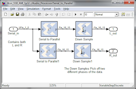
Audio comes in from the Audio Codec as stereo audio in a serial data stream. The left channel is the Mic input, and the right channel can be, say, a Line input.
This serial data is transformed into left and right channel 16-bit parallel data by the Serial_to_Parallel subsystem:
Audio_Processor -- Serial_to_Parallel:
(Click on image to enlarge)
Audio_Processor -- TX Equalizer:
The next block in the TX audio chain is the TX Equalizer. Dick added it because he wasn't satisfied with how his EV-664 mic sounded through the radio -- he thought his Astatic D-104 sounded much better, and so he decided to add an EQ stage to "perk up" his EV-664 microphone's response.
(This radio has a useful feature that allows the operator to monitor their TX audio and thus discover how a mic sounds and how for example, the information filter affects audio quality.)
The TX Equalizer is shown, below:
(Click on image to enlarge)
This is a 64-tap FIR filter, with coefficients downloadable via the radio's Command Interface from the user's control panel.
The 26-bit words from the Command Interface also contain a bit to select Line or Mic input, and another bit to Activate (or bypass) this equalizer.
Here is a look "under the mask" of the n-tap FIR filter that is the heart of this equalizer.
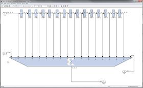
(Click on image to enlarge)
Audio_Processor -- OVL_Detect:
There is an Overload Detector which monitors the input to, and the output from, the TX Equalizer filter. If either are greater than half of full scale, an overload (potential overload, actually), is flagged.
(Click on image to enlarge)
AGC_and_More:
Next the TX Audio goes to the AGC block. The purpose here is to take a mic signal that might be low and, with the AGC circuit, amplify it up so that it approaches the full-scale range of the system.
You've seen this block already, above, in the receiver description. I've highlighted it, below:
(Click on image to enlarge)
Within this block we see the usual suspects:
(Click on image to enlarge)
And here is the path that the TX audio takes:
(Click on image to enlarge)
Let's take a quick look at the AGC block, highlighted below:
(Click on image to enlarge)
Below is the TX audio path through this AGC block:
(Click on image to enlarge)
I've also highlighted (in orange) a control signal which limits the maximum gain that can be applied to the mic signal (to prevent, say, background noise picked up by the mic from being amplified up to an annoying level).
AGC Xilinx -- Sequential Divide:
The highlighted circuit below controls how much gain can be applied to the TX Audio signal.
(Click on image to enlarge)
The smaller the divisor is, the greater the gain will be. The circuit above limits this gain by checking the divisor's value and, if the divisor is less than a value set by the operator, the divisor is limited to that value set by the operator. That is, this circuit essentially acts as a floor to the divisor value, preventing it from going below a level selected by the user.
There are four levels selectable by the user, each representing a change of gain by a power of 2 (6 dB) from the next.
AGC Xilinx --S-Meter:
Here's the S-Meter circuit that creates a PWM signal to drive an external analog meter.
(Click on image to enlarge)
In CW mode the PWM represents the TX Level (which controls the output TX power) of the CW signal.
In SSB/AM modes the PWM represents the level of the TX audio, and it does this by using the AGC divisor value (which, in the case of my AGC, is essentially just a leaky-peak detected copy of the audio coming into the AGC block).
If this audio is too high (i.e. greater than 0.5, identified by either bet 24 or 23 of the divisor being high), the PWM signal will be its highest value (31) and the external analog meter should point to its highest level, e.g. full scale.
Divisor values (and thus audio levels) below this peak value will be directly translated into one of 31 PWM levels using the next lower 5 bits of the divisor (bits 18-22)
TX Audio Select:
TX Audio next moves from the AGC block to the TX Audio Select subsystem block, highlighted below.
(Click on image to enlarge)
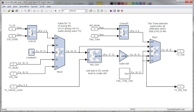
This block selects the audio source.
(Click on image to enlarge)
Specifically, the sources are:
- Zero (in Receive mode)
- Tx_Audio (SSB Transmit)
- CW_Oscillator (CW Transmit)
- TX_Audio summed with TX_Carrier_Level (AM Transmit)
- Two-Tone Generator (to test linearity of TX chain).
Note that TX_Carrier_Level adds a DC offset to the TX_Audio signal for AM modulation, and its value should be at least equal to the peak value of the TX_Audio. (If it is under then the AM signal will be over-modulated). In other words, this circuit generates the (DC + x(t)) term in the equation, below:
AM Modulation Equation
In the circuit, TX_Carrier_Level represents the equation's DC term, and Tx_Audio represents the equation's x(t) term.
And here's the Two-Tone source:
(Click on image to enlarge)
Time_Share_MPY:
The Time_Share_MPY block controls the level of the TX signal sent to the modulator and thence onward to the DAC. I've highlighted it, below:
(Click on image to enlarge)
And here is its circuitry:
(Click on image to enlarge)
Over_Modulation_Detector:
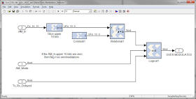
The final subsystem we will look at is the Over_Modulation_Detector subsystem, shown below:
(Click on image to enlarge)
This circuit is used in AM mode to detect if AM is being over-modulated.
(Click on image to enlarge)
Its operation is straightforward. In AM mode, the Transmit Audio signal from the TX Audio Select block represents the (DC + x(t)) term in the AM Modulation equation, listed here earlier, above. This term should never go below zero and should always be positive. If the Transmit Audio signal, in AM mode, does hit zero, then it is assumed to be over-modulating.
That's the end of this post! Notes follow...
Single-Pole Low-Pass IIR Digital Filter notes...
Realization of single-pole IIR filters:
I was curious about Dick's one-pole low-pass IIR filter (it wasn't in a form with which I was familiar), so I decided to dig a bit deeper...
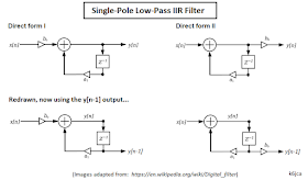
Dick's low-pass IIR filter can be thought of as a variant of the Direct Form II digital filter, but in which the y[n-1] tap is used as an output, rather than y[n], as I've shown in the drawing, below (lower right-hand corner filter).
(Click on image to enlarge)
Many readers might be familiar with the common Direct Form I realization of a single-pole low-pass filter that uses the y[n-1] output, shown in the lower left-hand corner of the drawing above. This was the form that I was familiar with and had seen (and used) many times over the years, and Dick's use of the Direct Form II realization initially confused me, until I realized it was equivalent to the Direct Form I.
Another point to note: with this type of single-pole low-pass filter, a1 and b0 often have the following relationship:
a1 = 1 - b0
and where a1 defines the decay-rate (or time-constant), which is the number of samples it takes to reach 36.8% of the original value according to the relationship:
n (samples) = -1/ln(a1)
So, for example, an a1 value of 15/16 will have a time-constant of about 16 samples. Therefore, if a unit step-function were applied as an input signal, it would take about 16 samples for the output to reach 63.2% of its final value.
Derivation of Time Constant:
I was curious as to the derivation of the Time-Constant formula: n = -1/ln(a1).
With some poking around the internet (e.g. here) and some pencil pushing, I came up with the following derivation:
Continuing on, let's now solve for n...
The Relationship of a1 and b0:
Another question I had: must a1 always equal 1 - b0 ?
The short answer is: no, a1 does not need to be equal to 1 - b0. If this equation is not satisfied it just means that gain (or attenuation) has been applied to the filter, but the filter's time-constant and low-pass response cut-off frequency remain determined by a1.
For example, let's take a low pass filter whose coefficient are: a1 = 15/16 and b0 = 1/16 (thus satisfying the equation a1 = 1 - b0)...
Now, suppose that prior to this low-pass filter we inserted a gain-stage whose gain was, say, 32:
Being a linear system, this additional gain of 32 can be combined with the b0 of 1/16 for an overall gain of 2. In other words, the circuit now appears to be an IIR filter with a b0 of 2.
Our equation a1 = 1 - b0 is no longer satisfied, but clearly the filter's low-pass filtering characteristic should not have changed, because applying gain in the signal chain prior to (or after) the filter should not affect the filter's filtering.
The same principle applies to Dick's use of the Direct Form II realization, in which the b0 coefficient is at the output, rather than the input, of the filter. Changing b0 essentially just adds gain (or attenuation) to the signal path.
Time Constants:
Some useful Time Constants for this radio (whose audio sample-clock period is 0.1024 ms), calculated using n = -1/ln(a1):
(Some internet digital IIR references:)
https://en.wikipedia.org/wiki/Digital_filter
http://www.dspguide.com/ch19/2.htm
http://www.eas.uccs.edu/~mwickert/ece2610/lecture_notes/ece2610_chap8.pdf
Background Notes:
SDR Notes: Weaver Modulation and Demodulation
SDR Notes: The Mixer Mathematics of Digital Down Conversion
Posts in this Series:
Part 1: Overview
Part 2: FPGA Modulation and Demodulation
Part 3: Interpolation and Decimation Filters
Part 5: Control Interface, Etc.
A Discussion on the Automatic Gain Control (AGC) Requirements of the SDR-1000, Phil Harmon, VK6APH. (Available for download from the FlexRadio website: here).
Standard Caveat:
I or Dick might have made a mistake in our designs, equations, schematics, models, etc. If anything looks confusing or wrong to you, please feel free to comment below or send me an email.
Also, I will note:
This design and any associated information is distributed in the hope that it will be useful, but WITHOUT ANY WARRANTY; without even the implied warranty of MERCHANTABILITY or FITNESS FOR A PARTICULAR PURPOSE.

















No comments:
Post a Comment