Thinking that this might become an issue, I thought I would change the connector type to N by using N-to-SMA adapters.
But I wanted to ensure that the weightier N-connectors (and whatever might be
attached to them) were not physically supported only by the NanoVNA’s SMA
connectors themselves. That could increase the chances of future SMA
connector failure.
So I purchased two N-to-SMA bulkhead adapters, and, after they arrived, I made
a simple chassis from PCB stock onto which to mount both my NanoVNA and the
two adapters:
I used two pieces of copper-clad PCB stock. One piece (double-sided) serves as the bottom plate onto which the NanoVNA
attaches (using 4 screws -- these screws are longer than the stock ones used
to attach the NanoVNA’s back cover).
The original back cover is still attached (so that I wouldn’t lose it) – you
just cannot see it.
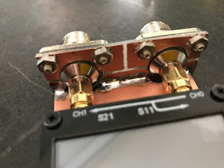
The second piece of copper-clad is single-sided, and upon it the two N-to-SMA
bulkhead adapters mount. I chose
single-sided stock because, on the NanoVNA PCB itself, the grounds for the two
SMA connectors split apart, and I wanted to continue this “separate-ground”
approach out to the N adapters and their mounting hardware.
Thus, if you look at the next two pictures, you will see how each N-connector
has its body and mounting hardware isolated from the other N-connector as well
as from the ground-plate holding the NanoVNA.
No conductive copper on the front side:
And mounting hardware isolated on the backside. (I used a Dremel tool with an
engraving bit to create the copper "islands", but you could use an Xacto
knife, too. It’s just a bit more work.) Note that only two screws
hold each adapter to the front plate.
If you look closely at the photo, above, you’ll see the solder-seam connecting
the two boards. There is an
identical seam on the other side of the bottom plate, as you can see in the
photo, below:
Solder on both sides makes this joint mechanically rigid, relieving any
mechanical stress on the NanoVNA's SMA connectors.
By the way, the only change I made to the NanoVNA, itself, was to use slightly
longer screws (I believe the thread size is M2.5, but don’t quote me!).
That's it! Hopefully this will spur your own ideas!
Standard Caveat:
As always, I might have made a mistake in my equations, assumptions, drawings, or interpretations. If you see anything you believe to be in error or if anything is confusing, please feel free to contact me or comment below.
And so I should add -- this information is distributed in the hope that it will be useful, but WITHOUT ANY WARRANTY; without even the implied warranty of MERCHANTABILITY or FITNESS FOR A PARTICULAR PURPOSE.


6 comments:
Good idear to make an adapter plate, but i would have used bnc as they require the least amount of force when changing leads.also you didnt need to remove the copper between the connectors, they have to have a good ground between them.
By only using 2 screws on each connector you will be still be applying forces to the smaller connectors but lengthways as the n connector tilts downward. N connectors do require force to tighten, and over a long period of time the male connectors get a dirty oxidised layer build up on the rubber internal seal that can become conductive at high freq..... Bnc's are in practice far better.. And keep the weight down. And fine for 900mhz
F5vhz
Thanks for the comments, Colin.
I'd actually first considered using BNC's, but because my feedlines are commercially-manufactured coax cables terminated with N connectors, I decided to go with those, instead. I have a plenty of BNC-female to N-male adapters, should I want to use BNC cables, instead.
Ground isolation at the N connector plate follows what appears to be the PCB layout philosophy, where CH0 and CH1 grounds are isolated (at least on the outer PCB layers). Perhaps to minimize undesirable inter-channel coupling via ground? It does not hurt to continue this isolation philosophy out at the N connectors.
As for two versus four screws per connector, I haven't seen any undue stress, myself, but I appreciate your bringing it up.
73,
- Jeff, k6jca
It seems that isolated grounds are dependent on the version of the PCB.
My version has them connected.
The best part of ham radio is repurposing and improvising. In the best tradition of MacGyver. I salute you for this clever elegant solution. When I opened my NANO my second thought was “how do I connect this to 8X coax. Thank you OM.
De NY2RF
Have you made calibration plugs to fit? Was thinking of doing same thing with pl259 plugs, then calibration came knocking on door! So have left unfinished
I have a set of N cal standards that I can use.
Post a Comment