This post is part 2 of my HP 3314A Function Generator
troubleshooting posts, in which I continue troubleshooting my swap-meet find.
Part 1 is
here.
Battery Replacement:
The HP 3314A contains a Lithium battery to keep power applied to the CMOS RAMs
(U211 and U212) and to the Reset Circuitry (U203, an MC14584B Hex Schmitt
Trigger IC) when the 3314A is powered off.
The image below shows the dead battery that was in the 3314A when I
purchased it. Although not easily seen in the picture below, there are
two wires attached to the PCB that are pushed against the ends of the battery,
but they are not soldered to it. So electrical contact with the
battery's terminals depends upon the physical pressure of the two wires
against the battery's ends.
My guess is that the two wires attached to the PCB wereleads that were part of
an older, originally installed by HP, battery, and a previous owner simply
clipped these two leads from the ends of that original battery and then
pressed them against the terminals of a modern replacement battery that did
not have wires attached to it, hoping that this physical contact would provide
a reliable electrical contact.
I purchased a CR123A battery holder and new 123-style Lithium 3 volt battery
via Amazon and, after removing the original two wires on the board, I used two
new wires to connect the holder to the PCB. This assembly is held in
place with a tie-wrap.
ROM Failure:
Even with the bad CMOS RAM temporarily replaced (see
Part 1), the
unit would still end up with a blank seven-segment display after the power-up
count-down sequence. Why was the microprocessor failing to continue?
Perhaps there's another memory failure.
Fortunately, HP included a number of self-tests in the HP 3314A. One of
these is a memory test, which verifies the contents of the ROM memory (of
which there are six ROMs in my early version of the 3314A (U207-U210, U236,
U238)), as well as the RAM (U233, U234) and CMOS RAM (U211, U212; these last two being
the battery backed-up RAM).
This memory test can be invoked by holding down the ARB button while turning
on the 3314A. It can take 20 to 30 seconds to complete, and, when
finished, it will display which memory devices test GOOD by turning ON a
front-panel LED for each good device. If the associated LED is OFF, then
the memory device failed the test.
When I invoked this test, the AMPLITUDE LED remained OFF, signifying
that U236 was bad.
(Note -- when I first tried to invoke this test, prior to replacing U212 (the
bad CMOS RAM IC), all of the LEDs would turn OFF and the test would never
finish.)
Pinout-wise, the six on-board ROMs seem equivalent to 2364 ROMs. These
are 8Kx8 bit memories. I have 2764 EPROMs in my junk box (from
designs I did 40 years ago) that are also 8Kx8 devices. Could I program one of my EPROMs to replace the bad on-board ROM?
But first, were the 3314A ROM binary
files even available?
So binary files were available, but one more issue remained -- the
original ROMs were 24 pin devices, but the 2764 EPROM is a 28 pin device.
I could wire up an adapter board, myself, but fortunately, one can purchase
adapter boards for this purpose, and eBay had just the thing.
(Apparently this was a common modification for the Commodore computer --
search for "2364 EPROM Adapter").
Here's a photo of the adapter kit I purchased from eBay (this photo is from
the eBay listing):
Note that pin 27 of the 2764 EPROM (its /PGM pin) should be tied to VCC for
normal READ operations. This pin is not normally tied high on the adapter board, but the board does include pads to accomplish
this -- I simply applied a solder-short from the "A14" pad to the "VCC" pad
(these pads are visible in the center of the board in the image, above).
Pin 26 of the 2764 EPROM should remain floating (No Connection). Note
that this pin corresponds to the "A13" pad on the adapter board, and it should remain unconnected.
With the adapter built and an EPROM programmed (using an inexpensive TL866A
PROM Programmer, available, for example, via Amazon), I soldered the adapter
to the PCB in place of the original ROM and inserted the programmed PROM into
its socket.
I powered up and...hurray! The seven-segment display did not blank out after the initial count-down following power up!
And when I invoked the Memory Test at
power-up, all memories passed.
But there were still problems -- now the unit displayed the following errors
during its power-on calibration procedure:
E30 (No Frequency Detected)
E34 (Signal Amplitude Outside Measurement Range)
So on to the next problem...
Error E30: No Frequency Detected:
The Service Manual has a flowchart for troubleshooting Frequency Calibration
errors. Following this chart led me to the box labeled "Common Mode
Rejection Circuitry":
The Common Mode Rejection Circuitry is part of the "Triangle Integrator"
schematic, below. The purpose of this circuitry is to keep the DC level
at the Source Pins of Q220 (i.e. pins 1 and 5) at about -5 Vdc.
On my board I measured the "Common Mode Sense" voltage (at the base of Q211)
to be -3.4 volts, not the specified -5 volts. Clearly there was a
problem. But was the problem actually with the common-mode circuitry, or
was it somewhere else, with the symptoms exhibiting themselves as a
common-mode problem?
(Important Sidebar Note: Although the Service Manual shows voltages at
Q220 pins 1 and 5 having a DC offset of -5 Vdc (Waveform 1, Figure 8-15,
although good luck discerning this level from the manual download from the
Kesight site), these two voltages can actually be a bit lower than -5 Vdc
(e.g. -5.4 Vdc), due to Q211 base current, even if the "Common Mode Sense"
signal at the base of Q211 is -5 Vdc)).
But back to the problem -- why was the Common Mode Sense level so far off?
First, I needed to understand the circuit, starting with the Triangle
Integrator circuitry.
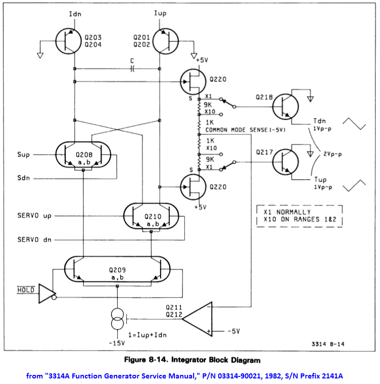
The functional operation of the Triangle-wave generator can be understood
using the block diagram, below.

First, note that in normal operation (e.g. the generator's state after power-up), the path through the Q210 differential pair is not used. Instead, Q208 controls the generation of the triangle wave.
Basically, a constant current is passed through the capacitor C (connected
across the collectors of the two differential pairs Q208 and Q210), first charging the
capacitor in one direction (Iup and Idn both passing through, for example, the left-hand transistor of the differential pair, Q208a, with Iup charging the capacitor).
A downstream comparator (not shown in the block diagram, above), monitors the voltage across the capacitor and, when this voltage reaches a threshold, it flips the states of the Sup and Sdn control signals, forcing the capacitor to charge in the opposite direction (i.e. via Idn, with both Iup and Idn now passing through Q208b).
If everything is working properly, this flipping back and forth of the charging path should result in a 1 volt
peak-to-peak triangle waveform at the output of the Triangle Integrator
circuitry (i.e. 1 Vpp at the emitter of Q217 and 1 Vpp at the emitter of Q218).
And because Q217 and Q218 are emitter followers) the same peak-to-peak
levels should be seen at each of Q220's two Source pins (pins 1 and
5).
But when I measured the signals at Q220's Source pins, there wasn't a
1 Vpp signal present on either pin. Instead, one Source pin (pin 1) was stuck at 0.7 Vdc, while the other Source pin (pin 5) was sitting at -7.5 volts.
The voltage delta between these two pins was 8.2 Vdc (much greater than the
1 volt delta it should have been). And it was because of this excessive voltage delta that the Common Mode Sense voltage measured to be -3.4 Vdc
and not the desired -5 Vdc (the Common-Mode Sense voltage, assuming that Q211's base
current is insignificant, is a function of the voltage divider consisting of R233, R234, R237, and R23 connected in series between the two Source pins of Q220, and thus this voltage should equal the average of the voltage between these two pins (i.e. (0.7 + (-7.5))/2 = -3.4 V).
So why was the voltage delta between the two source pins so large? And
why weren't the transistors in the Q208 differential pair flipping back and
forth to create the triangle wave? Was there a problem with the triangle generator, or maybe the comparator?
This was looking a lot less like an issue with the Common Mode Rejection circuitry and instead an issue somewhere else.
Probing the circuit's transistor voltages gave me some very strange results when I looked at transistor voltages in aggregate, but after digging a bit further I found that my confusion was, in fact,
caused by a schematic error in which the transistor reference designators
for Q208a and Q208b were swapped, compared to the labels on the PCB
silkscreen. The correct reference designators are shown, below:

With that schematic issue resolved, the measured Integrator's voltages now made
sense, and the problem would seem to be further downstream, at the
comparator. (It is the comparator that flips the Sup and Sdn signals
back and forth, which in turn control the charging direction of the
integrating capacitor via Q208a or Q208b).
While troubleshooting the comparator's voltages I ran into another documentation error
-- this time in the Comparator Block Diagram:
(And although it is not shown in this blog post, Figure 8-19 has the same pin
errors.)
As I probed the DC voltages of U303 (a CA3102 dual differential amplifier IC)
it quickly became apparent that something was really messed up. For
example, the device's Substrate pin (pin 5) was sitting at -4 Vdc instead of
-15 Vdc. The substrate pins voltage should be the lowest voltage on the chip, and it clearly was not (see the voltages in the image, below).
Also, the current into pin 11 (transistor base current) was a whopping 33 mA!
It looked like U303 was bad, but I didn't have any replacements in my
junkbox. Fortunately, I found some on eBay and ordered a couple.
But in the meantime I decided to make a simple replacement for the CA3102
using six discrete 2N3904 transistors to replicate the CA3102's two
differential amplifiers. It wouldn't be perfect -- the 2N3904
transistors weren't matched and their fT is much lower than that of the
CA3102's transistors, but hopefully I could continue with my troubleshooting
while awaiting the arrival of the CA3102 devices.
(Sidebar: Interestingly, the CA3102 was already mounted in a socket. I don't know if HP did this during manufacturing, or if someone later modified the board and added the socket. If the former, maybe the CA3102 devices needed to be hand-selected to get the required performance.)
Below is an image of my "Temporary CA3102" replacement, using six 2N3904
transistors and built onto a 14-pin DIP header that, in turn, is plugged into
a 14-pin socket at U303's location on the PCB:
With this temporary replacement installed on the PCB, there were no longer any
"E30" errors at power up, and there was now a sine wave present at the 3314A's
output!
But, even though there was now a sine wave output, there were still errors
displayed at power up. These errors consisted of one E31 error
(frequency error exceeds correction capability) and four E34 errors (signal
amplitude outside measurement range) that were displayed during the
calibration sequence.
So on to the next problem...
Error E34: Signal Amplitude Outside Measurement Range:
Error E34 identifies the signal amplitude as being "outside measurement
range." But what is "outside measurement range"?
Unfortunately, the Service Manual seems to be mute on this error condition,
but, if I measured the 3314A's output (across a 50 ohm load) with the 3314A's
amplitude set to 1.00 volts (peak-to-peak) and 0 volts DC offset, the output
level and offset were clearly not what they should have been, as the image
below shows:
With the output amplitude set to 1.00 volts and no DC offset, the voltage
across a 50 ohm load measured to be 0.88 Vpp with an offset of -0.24
Vdc, not the desired 1.0 Vpp with 0 Vdc offset.
Clearly there was a problem.
Because E34 is an "Amplitude Calibration" error, I decided to follow the
Service Manual's "Amplitude Calibration Troubleshooting Flowchart" (figure
8-11B).
Following its flow and making the recommended measurements at the appropriate
steps, I arrived at its conclusion that, "Maybe U502 or associated
cells/circuits" were at fault.
Well, that's pretty vague.
And what is U502? It is HP's custom "Sine Shaper" IC that converts the
triangle wave into a reasonable facsimile of a sine wave. If this part
were bad, then I might as well abandon the project, because it was sure to be
"unobtanium."
But it was too early to abandon hope, so I started troubleshooting by first
examining U502's signals.
Well, U502's signals "seemed" good, in the sense that nothing was obviously
out of whack, but there wasn't much information in the Service Manual as to
what U502's signals should actually look like.
Assuming (hopefully) that U502 wasn't the issue, could the problem be in an
earlier stage? For example, I had noticed that the DC levels at the
Integrator circuit's Q220 Source pins were about 0.4 volts lower than the
image for the waveforms shown in the Service Manual (i.e. they measured at
-5.4 volts instead of -5 volts), as shown, below:
Could this offset be the problem? A quick test (raising the Source
voltages of Q220 from -5.4 to -5 volts by paralleling R219 (in the Q211, Q212 circuit)
with a variable resistor) showed that changing this DC offset had absolutely
no effect on the 3314A's output voltage level or offset.
Hmmm, could the problem be in the next stage, the Transconductance Amplifier?
Did not seem so. DC voltages seemed reasonable, and signal levels at the
bases of Q203 were correct.
So the signals going to the Sine Shaper seemed to be reasonable, at least as
far as I could determine (which was not very far).
Again, hoping that the Sine Shaper IC was not the issue, perhaps the problem
was in a stage following it.
The Sine Shaper drives the "Preamplifier" Stage (Figure 8-23 in the Service
Manual), which in turn drives the "Output Amplifier and Step Attenuator"
stage, whose output, in turn, goes to the output connector on the front panel.
As I measured the DC levels of the Preamplifier from input to output, they
looked OK...but wait! The node common to R611, R612, R606, R607, and
R608 measured at 0 Vdc (which makes sense, as this should be the DC level of a
balanced amplifier when there is no DC offset), but the DC voltage at the
other side of R607 (i.e. at connector J1 to the Output Amplifier's
input) was at -0.24 volts.
What happens to the DC level at the Preamplifier's J1 connector if I
disconnect the cable between J1 and the input to the Output Amplifier?
The DC voltage at the output side of R607 goes to 0 Vdc, and the sine wave
amplitude increases such that, when this point is terminated with 50 ohms, its
amplitude is correct.
That is, with the Preamplifier's output disconnected from the input of the
"Output Amplifier" stage, and with the 3314A's amplitude set to 1 Vpp and 0
Vdc offset, the sine wave at the Preamplifier Output (terminated with 50 ohms)
correctly measures to be 1 Vpp with 0 Vdc offset, instead of the 0.88 Vpp with
-0.24 Vdc offset that would have been measured at the output of the
Output Amplifier.
So the Output Amplifier would seem to the be culprit! Here is an image
of that board:
While probing the Output Amplifier's DC voltages, it quickly became
apparent that Q10 was bad (an MPSH10 NPN transistor -- its Vbe measured to be
3.7 V).
I replaced Q10 and powered up the unit. Success! There were
no longer any E34 errors during power-on calibration.
Important Note: The scanned copy of the schematic for the "Output
Amplifier and Step Attenuator" board in the downloadable Service Manual on the
Keysight site (see Resource list, below) is missing some circuitry, which I've
shown in the image, below (copied from a later manual revision):
Conclusion:
With all fixes installed, the 3314A's Calibration Sequence (initiated at
power-up) successfully completes with no displayed errors. And it plays the Hallelujah Chorus! (See
here for an example).
I have not done any of the Performance Tests listed in the Service Manual. I might do these at some future date, at which point, if there are any issues that need repair, there might be a Part 3 added to this 3314A troubleshooting series.
Finally, note that all troubleshooting was done without the benefit of a Signature
Analyzer. However, if there had been problems with the digital logic, a
Signature Analyzer (e.g. HP 5004A) would have been invaluable.
Other Notes and Comments:
1. E31 Error:
The E31 error (that began appearing during the Power-up Cal sequence after I
had replaced the bad U303 (CA3102) with my temporary "six 2N3904"
replacement), disappeared when I replaced the U303 temporary fix with an
actual CA3102 device.
2. Replacing the CMOS RAM with higher-current devices:
If uPD444 CMOS RAMs are not available for replacing U211 and/or U212, other
1Kx4 devices can be used, if they are pin compatible. Note, though,
that if the new RAMs require higher Vcc current, then to prevent battery drain their power pins should not be attached to their respective pin 18 PCB pads (which are powered by the battery when AC power is OFF).
Instead, lift the power pins (pin 18) of the two devices and connect these
two lifted pins to +5 Vdc at the "front-panel" side of C17, as shown in the image, below
(the example, below, uses two Intel D2148H RAMs in lieu of the two original NEC
uPD444 RAMs):
With this modification, the CMOS RAM will no longer retain stored information when the 3314A is turned off. And thus there will be an "E09" error (non-volatile
memory lost; battery down), displayed at the end of the Power-up calibration
sequence, every time the 3314A is powered up.
Resources:
HP 3314A Manuals: https://www.keysight.com/us/en/support/3314A/programmable-function-generator.html
HP 3314A Repair in 3 parts: https://diysquared.blogspot.com/2021/04/fixing-hp-3314a-function-generator-part.html
HP 3314A Repair on YouTube: https://www.youtube.com/watch?v=wNxgBubSfH8
HP 3314A Repair (on Antique Radios forum): https://antiqueradios.com/forums/viewtopic.php?f=8&t=360491
HP 3314A Teardown (EEVblog): https://www.eevblog.com/forum/testgear/hp-3314a-function-generator-teardown-explanation/
HP 3314A Playing the Hallelujah Chorus: https://www.youtube.com/watch?v=H90d6sPUF6A
(Note: Hold down FUNCTION (the blue key), SW/TR INTVL, and
START FREQ while powering up the unit).
HP 3314A ROM Images: http://www.ko4bb.com/getsimple/index.php?id=manuals&dir=01_ROM_Images_and_Drivers/HP_3314A_Eprom
Standard Caveat:
As always, I might have made a mistake in my equations, assumptions,
drawings, or interpretations. If you see anything you believe to be in
error or if anything is confusing, please feel free to contact me or comment
below.
And so I should add -- this information is distributed in
the hope that it will be useful, but WITHOUT ANY WARRANTY; without even the
implied warranty of MERCHANTABILITY or FITNESS FOR A PARTICULAR PURPOSE.