Summary:
My "stock" IC-725 transceiver's frequency drifts over time (significantly if one is operating any of the newer digital modes). To improve stability, I made the following modifications to my IC-725:
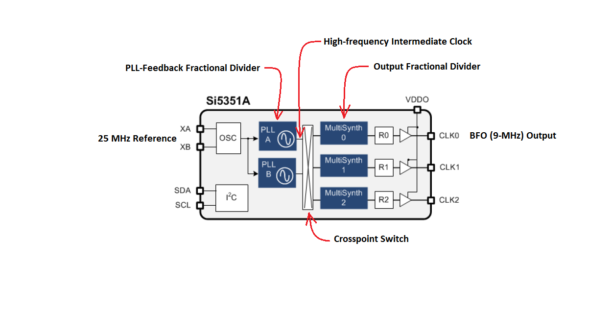
- Change the 9 MHz BFO from the stock crystal oscillator instead to a BFO generated with an Si5351A Clock Generator IC on a pre-fabricated development board. (The Si5351A, using one of its outputs, generates the four different BFO frequencies required for different modes of operation.). The Si5351A is clocked with a Temperature-Compensated Crystal Oscillator (TCXO) in lieu of its normal 25 MHz crystal reference.
- Change the 30.72 MHz Reference Oscillator from the stock crystal oscillator to an Icom CR-64 "High-Stability Crystal Unit", and power its heater via regulated +12 VDC (instead of the radio's 13.8 VDC supply) by adding a LM2940-12 low-dropout regulator to the transceiver's "PLL Unit" PCB.
- Change the fan from only being on during Transmit to always being on anytime the radio is ON (to eliminate internal-to-the-radio temperature excursions over a relatively short period of time that might affect oscillator frequencies).
I wanted to have a dedicated WSPR radio that could be controlled by a Raspberry Pi computer. Searching the shack, I dug up an Icom IC-725 radio that I had purchased new back in the late 80's (or early 90's), when I was getting back into ham radio.
It has a computer-control interface that I could drive with a USB adapter connected to the Raspberry Pi, and so it seemed to be the ideal rig. And it hadn't been used for years, so why not put it back to work?
But when I attempted to make WSPR contacts with it, my reported drift-rate (as reported by stations copying my transmitted WSPR signal) was 4 Hz/minute! Ouch!
Clearly, my stock IC-725 was not up to the task. Which got me thinking...could I improve it?
IC-725 Oscillators:
There are two oscillators in the IC-725. One is a 30.72 MHz oscillator used for frequency conversion (on the "PLL Unit" PCB), and the other is the BFO oscillator that operates around 9.01 MHz (actual frequency depends upon the mode of operation).
Both oscillators use crystals, but the BFO changes its frequency by switching various inductors and capacitors in series with the crystal to pull its frequency one way or another, depending upon mode.
Measurements I made showed both oscillators drifted appreciably over time and both oscillators would need improving.
Improving Frequency Stability of the 9.01 MHz BFO:
The BFO switches between the following frequencies, depending upon mode:
- USB: 9.0130 MHz
- LSB: 9.0100 MHz
- CW(Rx): 9.0098 MHz
- CW(Tx): 9.0106 MHz
- AM/FM: BFO Off
An obvious choice was to eliminate Icom's method of switching inductors & capacitors to vary the oscillator frequency and instead to replace it with a more modern part, the Silicon Labs Si5351 Clock Generator.
To make my task easier, I chose Adafruit's pre-assembled breakout board with an installed Si5351:
BFO Generation using the Si5351, Hardware:
BFO hardware changes consist of modifications made to the radio circuitry plus the addition of a separate Arduino/Si5351 clock-generator daughter-board.
First, the daughter-board description...
Clock-generator Daughter-board:
I wired a small daughter-board (to mount behind the radio's front panel) with an Arduino NANO processor and the Si5351 clock generator circuitry. The Arduino monitors the IC-725 "mode" signals and, depending upon their state, programs the Si5351A to generate the appropriate BFO frequency.
The Si5351A came pre-assembled on a small PCB. I replaced its "stock" 25 MHz crystal a 25 MHz TCXO to improve frequency stability over temperature. (Note that the Si5351A is not spec'd for use with an oscillator module such as the TCXO I am using. More on this later in the post.)

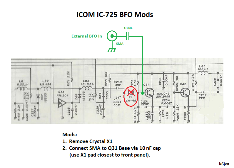
Schematic Notes:
- Note that the crystal at location Y1 must be removed from the Adafruit Si5351 board. U4, a 25 MHz TCXO, now provides the frequency reference for the Si5351.
- The control signals to the Nano from the IC-725 (USB, LSB, CW, and RX) have logic-high levels equal to 8 volts. Therefore, voltage dividers (each consisting of a 3K and a 4.7K ohm resistor) to bring the levels into spec with the Nano's input requirements.
- Per the CTS datasheet, pin 6 of the 25 MHz TCXO (U4) should be filtered with a 100 nF capacitor. However, note that the part I am using is not one whose frequency can be "voltage-controlled". It's not clear if this capacitor is still required, but I installed it anyway, just in case.
- Resistors R13 and R14 form a simple voltage divider to bring down the output level of the TCXO prior to its connection to the XA pin of the Si5351. C12 rolls off the higher frequencies of the TCXO's square wave, and C13 capacitively-couples the signal to the XA input.
- Capacitors C6-C9 provide one-pole EMI filters in conjunction with the input voltage-divider resistors, to reduce any RF that might be coupled onto these wires.
- If U4's 25 MHz frequency shifts with aging of the oscillator, the Arduino software can program the Si5351 to offset this aging.

3. The BFO frequency depends upon the state of the USB, LSB, CW, and RX signals, as follows:

Si5351 9 MHz BFO Spurs:
There are spurs on the 9 MHz signals, but, assuming the Si5351's output divider is set to an even number, the larger of these spurs lie outside the passband of the 9 MHz filters (i.e. they would mix with filter stop-band noise, rather than with within-the-filter's-passband signals). Thus, they shouldn't be a problem.
(See the Arduino Code section below for more detail on these spurs and how I minimized (but did not eliminate) them).
Improving Frequency Stability of the 30.72 MHz Oscillator:
I tried a number of different ways to improve stability of the 30.72 MHz oscillator. These included:
1. Using the Si5351A to generate the 30.72 MHz clock (abandoned due to, in my opinion, unacceptable spur generation).
2. Using a Voltage-controlled Temperature-Compensated Crystal Oscillator (VCTCXO). (Abandoned to due unacceptable frequency drift over time).
3. Using the Icom CR-64 High-Stability Crystal Unit (performance deemed acceptable after modifying the IC-725 to power this unit with regulated +12 VDC in lieu of the "unregulated" 13.8 VDC power to the radio).
(Note, the CR-64 is not an OCXO (Oven-Controlled Crystal Oscillator). It actually is just a crystal packaged with an oven that replaces the original crystal of the 30.72 MHz oscillator -- the rest of the oscillator's circuit is still the original circuit of the radio, outside of the CR-64, and thus C134 and L35 still adjust the oscillator's frequency.)
I'll discuss the issues with the first two methods listed above later in this post. Let's look at the method I finally chose:
IC-725 Modifications to the 30.72 MHz Oscillator Circuit:
Hardware modifications to the IC-725's 30.72 MHz Oscillator circuit are:
1. Remove the stock 30.72 MHz crystal (CR-21 on the "PLL Unit" PCB) and replace it with an Icom CR-64.
2. Change the DC power to the CR-64's heater pin:
- Lift the leg of L33 closest to C132 (47uF electrolytic).
- Solder LM2904CT-12 voltage regulator to the side of the oscillator shield wall.
- Add input and output capacitors to the LM2940.
- Connect the LM2940's input pin to the lifted-pin of L33.
- Connect the LM2940's output pin to the L33 PCB pad that had held the now-lifted pin.
3. Connect a 2-pin female header cable to the LM2940 +12V output and ground (this will supply +12 VDC to the Arduino board).

Notes on the IC-725 30.72 MHz modifications:
The LM2940, being a Low-Dropout (LDO) regulator, has specific requirements regarding the ESR and capacitance of its output capacitor. For regulator stability this cap must be at least 22 uF and its ESR should be within the ranges shown in the graph, below:
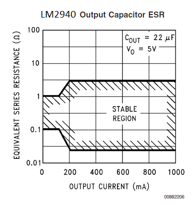
(Refer to the LM2940 datasheet for more details).
The oven of my CR-64 draws about 80 mA when powered with 12V (after it has warmed up). This current, in addition to the current for the Arduino and Si5351A should be less than 200 mA, so the ESR for the output capacitor should be in the range of 0.1 to 1 ohm to ensure regulator stability. I used a 22 uF tantalum capacitor from my junkbox whose ESR measured about 200 milliohms (measured on my HP 4274A).
(Note that this tantalum cap is in parallel with the 47 uF aluminum-electrolytic cap (C132) on the radio's PCB. So the equivalent-ESR will be lower, but not by too much -- Aluminum Electrolytic capacitors typically have significantly higher ESR values.
Never the less, I used my oscilloscope to verify that the output of the LM2940 had no oscillations.
Here's the implementation of the LM2940 circuit. Note that my IC-725 does not have a shield "cap" for the 30.72 MHz oscillator section.

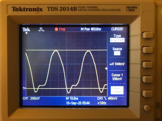
With the CR-64 powered by the radio's 13.8VDC supply (i.e. the "stock" connection for the CR-64), I discovered that there was some frequency drift (in one direction) during WSPR TX that would then drift back during RX, as shown by the screen captures, below. (The signal I'm monitoring is generated via my HP 3335A generator (with a short wire as an antenna at its output), set to 14.0972 Mhz (= 14.0956 MHz + 1600Hz) :


Discarded 30.72 MHz Oscillator Options:
Let's look at the two 30.72 MHz oscillator options that I discared:
1. Using the Si5351A to generate 30.72 MHz.
Generating 30.72 MHz using the Si5351A and its 25 MHz reference is a straight-forward task, given that the Si5351A has two internal oscillators and three outputs.
But fractional-division is going to occur somehow, and thus some amount of spurs will be generated. (I recommend that it be within the PLL feedback loop and not at the Si5351A's output -- set that divisor to be an even integer. I used the Si5351A's CLK2 output and I set its output divisor to 34).
Here's a look at the output spurs...
Si5351 30.72 MHz Oscillator Spurs:
Spurs on the 30.72 MHz oscillator could be a problem because, given the wide bandwidth of the input signal into the mixer assigned to it, spurs could cause undesirable mixing products to appear in the RX passband.
Close in spurs within +/- 10 KHz look great (20 KHz span):

If the span is increased to 1 MHz, spurs become more evident:

And even more so if the span is set from 1 to 100 MHz:

The spurs surrounding the 30.72 MHz fundamental could be a problem. When I connected an HP 8640B signal generator to the input of the transceiver, set the transceiver's receive frequency to 10.15 MHz and then started tuning the 8640B away from this frequency in either direction, I could hear spur products.
2. Using a separate VCTCXO for 30.72 MHz:
I had initially installed a TCXO to generate the 30.72 MHz reference-oscillator signal, but after I installed it I discovered it was too far off frequency, and so I changed the design to use a voltage-controlled TCXO (VCTCXO) with a 10-turn pot to control the oscillator's frequency.
Here are the spectrum plots of the Conner-Winfield T604-30.72M VCTCXO that I used.
First, 5 KHz span:


A Note Regarding the Use of an External Oscillator with the Silicon Labs Si5351A-B-GT:
Silicon Labs only specifies the Si5351A-B-GT part to be used with a crystal as its frequency reference. It does not specify the part for use with an external oscillator such as the TCXO I used -- it is only spec'd for use with a 25 or 27 MHz crystal as its Frequency Reference.
On the other hand, the Si5351C part is spec'd for use with an external oscillator as its frequency reference. However, the Si5351C is only available in an QFN package, and I have not yet found anyone who supplies a pre-fabricated development board for this part.
Therefore, for the design in this blog post, I am using a pre-fabricated development board (from AdaFruit) with an Si5351A and associated circuitry already installed upon it, and I have modified it to drive the Si5351A's crystal input with an external oscillator (TCXO) whose output has been modified to mimic the Si5351A's crystal-input signal.
This thread on the Silicon Labs forum highlights the issue of driving the crystal-only chip with an external oscillator: https://www.silabs.com/community/timing/forum.topic.html/si5351_msop10_packag-wocK
Note the statement that the part is only spec'd for use with a crystal.
But does this mean that an external oscillator can't be used? Perhaps not, as pointed out here.
But speaking as an engineer with 40 years of design experience, I would never intentionally design a product that did not follow a manufacturer's specifications -- doing so can lead to a product-support nightmare (for example, if the part's manufacturing processes changes and the part begins failing in my product) which would lead back to only one and only one root cause: me, and not the part manufacturer.
For this "one-off" design, though, I decided to take the risk. Why not make the TCXO's signal look similar to a crystal's signal at the XA pin of the Si5351A? Maybe this would minimize my risk of using the part outside of Silicon Lab's specs.
First thing to do -- measure the signals at the Si5351's XA and XB pins:

XB pin with xtal: Amplitude = 1.04 VPP.
Next, drive the XA pin with the TCXO (via a voltage divider, one-pole RC filter, and capacitively coupled):

XA pin with TCXO: Amplitude = 530 mVPP, DC Offset = 450 mV.

XB pin with xtal: Amplitude = 1.0 VPP.
Summary: the Si5351A XA and XB pin waveforms, with the TCXO, are similar to (but not exactly matching) those waveforms created with the original 25 MHz crystal.
One difference: note that the XA pin's waveform with the TCXO is similar to a square wave (but filtered by both the scope's response as well as the one-pole RC filter at the TCXO's output. Therefore the 25 MHz fundamental of the square wave will have a larger amplitude than what is shown, above, (probably on the order of 530mVPP*4/pi (the latter the ratio of fundamental amplitude to square-wave amplitude), or 670 mVpp).
So...the TCXO signal is not exactly the same at pin XA, but it is closer than if I were driving pin XA (capacitively coupled) with the 3.3Vpp square-wave from the TCXO's output.
For my own use, this seems to be good enough. But if I wanted to improve upon XA's waveform, additional filtering (and a change to the voltage-division ratio) could be applied to the TCXO waveform to bring it closer to that of the crystal-generated waveform.
Other Bits of Flooby-dust:
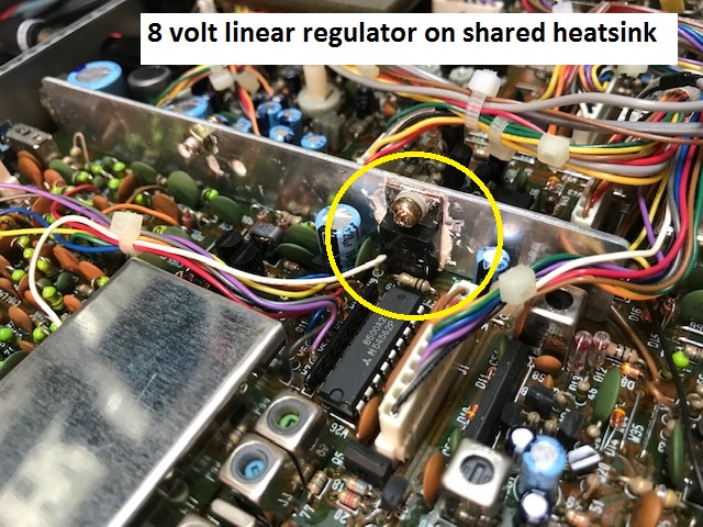
8-volt Regulator:
As I mentioned above (in the fan section) the 7808 8-volt linear regulator and its heatsink get hot. It sources about 0.25 amps (measured in CW mode), which means, given an input voltage of 13.8 volts, it's dissipating about 1.5 Watts of power.
I thought I would try replacing it with a 5V switching regulator (buck converter, found on Amazon) that I would convert to 8 volts:

The code on the IC package is AGCE, which corresponds to an MP2315 500-KHz switching regulator, and the board's circuit is very similar to the schematic (shown below) found on the Monolithic Power Systems website. (There are a few extra parts on the actual board, such as LED, TVS on output, etc., but, per the 3-letter codes on the resistor packages, the resistor values are almost all the same (note that R2 is 7.32K on the board rather than the schematic's 7.5K).

I removed the unneeded USB connector and cut off the unused PCB area to reduce its size. I then removed the TVS 5V over-voltage protection (connected to the board's output voltage node) and paralleled the on-board 7.32K resistor with 10.7K ohms to get about 8 VDC out.
But when I installed this board in the radio in lieu of the original 7808 linear regulator, I discovered that it generated noticeable EMI at 7.135 MHz (I only checked the 40-meter band), and so I removed it and reinstalled the original 8V linear regulator.
30.72 MHz Signal Level:
(Note: this discussion is for the now-discarded design using the VCTCXO)
When I started making my modifications I neglected to measure the original signal level of the 30.72 MHz oscillator (and I was too lazy to go through the effort of unhooking the cables from the board, removing it, resoldering the crystal onto it, then reinstalling the board and reconnecting all of the cables to it).
Instead, to determine what would be an adequate oscillator signal level, I used an HP 3335A signal generator set to 30.72 MHz and connected it to the SMA I had installed at the IC-725's for injecting a 30.72 MHz clock.
While listening to the audio of a received CW signal, I adjusted the signal generator's output from a low level until, to my ears, it seemed that the audio output level was no longer increasing.
This plateauing of audio output occurred when the 3335A's output was around +9 to +10 dBm.
Measuring (using my TDS 350 oscilloscope) the signal at J4 of the IC-725 (with P4 inserted) and +9 dBm of drive from the HP 3335A, the signal level was 740 mVpp (248 mVRMS using the TDS 350's RMS calculator).
When driven with the VCTCXO, the voltage at J4 measured to be 780 mVpp (267 mVRMS), putting it within my target goal of being equivalent to the 3335A output of +9 to +10 dBm.
30.72 MHz secondary oscillations:
(Note: this discussion is for the now-discarded design using the VCTCXO)
The VCTCXO drives the base of the oscillator's transistor in lieu of the 30.72 MHz that was originally in the circuit (I did this so that I would not need to remove many parts). I also removed the base-emitter capacitor, turning the circuit into an emitter-follower for the Si5351 signal.
While testing with the Si5351 generating the 30.72 MHz, I tried putting different filters (from Mini-Circuits) in series with the Si5351's output in an attempt to lower the spur content of the 30.72 MHz signal.
But, surprising to me, these filters had an undesired effect -- they caused the IC-725's oscillator to start oscillating again, but at a different frequency. And so there were two frequencies at the output of this oscillator -- the Si5351 frequency and a different (but fairly close) frequency.
What was going on?
Although I had removed the original crystal that was the frequency-determining component of the IC-725's oscillator, by connecting a filter in series with the Si5351's output to the base of the IC-725's oscillator transistor I was connecting a new resonant circuit (composed of the filter's inductors and capacitors) to the transistor's base, with the other side of the resonant circuit effectively connected to a low-impedance point (i.e. the output of the Si5351).
And even though I had removed the original base-emitter capacitor, the original oscillator circuit was now seeing the filter as a new resonant circuit in lieu of the original crystal and oscillating at the frequency determined by the filter's components.
In addition, the circuit's transistor was still acting as an emitter follower for the Si5351 signal. So it was self-oscillating as well as acting as a buffer for the Si5351-generated signal.
The fix -- remove the filter (and stop the unwanted oscillations) and replace the Si5351 with the VCTCXO (eliminate spurs around the 30.72 MHz signal).
Radio Stability with these Modifications:
At the moment the IC-725 has been running WSPR for a day and a half and I am satisfied with the improved stability of the IC-725. However, while monitoring my HP 3335A-generated 14.0972 MHz "marker signal" on WSPR, I have noticed a long-term drift of roughly 10 Hz over 24 hours.
And during this period, when the radio does drift, it's usually fairly quickly -- i.e. several Hz within, say, 2 minutes, and then it seems to stabilize and not change (or change imperceptibly) for a long time.
I haven't investigated if this drift is due to the CR-64 or due to the TCXO driving the Si5351. This would be done by also checking the frequency offset of a marker on, say, on the 10-meter WSPR band -- if the drift on 10 meters and 20 meters is the same amount (in terms of Hz), then the BFO is dominating drift. But if they are different, then the 30.72 MHz oscillator is dominating drift.
For the moment I'm assuming that it's the CR-64's crystal stabilizing over time, in the same way that an OCXO might take a few days to stabilize (as I've seen with my GPSDO's HP OCXO, when powered-up from a cold-start).
Future Modifications?
Because my 30.72 MHz VCTCXO modification is still in place within the radio (but with no power applied to it because I am now using the CR-64), one future modification might be to added a PLL circuit (such as the Analog Devices ADF4001 "Integer-N PLL" IC, plus filter) and lock the 30.72 MHz oscillator to my lab GPSDO frequency reference (for my Arduino-based GPSDO, see here).
Other Links of Interest:
Modifying an IC-751A for Digital Modes: https://squashpractice.com/2017/03/06/modifications-to-the-ic-751a-for-the-digital-modes/ (Note that the mods include replacing the stock 30.72 MHz oscillator with an OCXO and small switching power-supply module -- this is a mod I would have tried if I hadn't found a CR-64 (on eBay), but I would be concerned that EMI from the switcher might interfere with the radio).
Insulating the IC-746A's oscillator with cotton-wool balls: https://www.chris.org/Modifications/IC-746-almost-free-tcxo.html
Standard Caveat:
Also, I will note:
This design and any associated information is distributed in the hope that it will be useful, but WITHOUT ANY WARRANTY; without even the implied warranty of MERCHANTABILITY or FITNESS FOR A PARTICULAR PURPOSE.