This is the second post in my series of blog posts describing my 500 watt HF
Power Amplifier project:

The topic of this post will be the PA's Power Amplifier assembly, including its bias-voltage circuitry. I've circled this assembly in the block diagram, below:

As I mentioned in Part 1, this design is based upon a Microsemi app note (App Note 1819):

The two schematics contained in this app note are shown, below...


For convenience I've combined these two schematics into a single ORCAD schematic:

Comments on the Application Note:
The application note contains a wealth of information, and I strongly recommend reading it. Useful highlights (for me) include:
Note, too, that here are a few errors in the app note...
App Note Corrections:
There are a couple of errors/corrections in the App Note's parts list (Appendix 1 of App Note):

This photo (in the original app note) also shows C14 as an SMT device, but the part's list specifies an axial-leaded component.
Finally, there are a couple of pieces of info missing from the app note...
App Note Omissions:
Two significant pieces of information are missing from this App Note:
Other useful comments from the App Note author, Dick Frey, K4XU:
From my correspondence with Dick:
PA Testing, First Steps...
Would the design, as described in the app note, meet my goals (see previous post)?
The only way to determine if it was suitable would be to build it and test it. So, armed with the app note, parts, and PCB purchased from Express PCB, I began assembling.
But, I did make one change to the design:
I used VRF2933 transistors in lieu of the specified VRF2944 parts. I was able to purchase a pair of the VRF2933 FETs relatively inexpensively and their performance is similar to the VRF2944 (note that the Elecraft KPA500 uses VRF2933 FETs, too).
(I would later switch back to VRF2944 transistors, but more on that, later...)
When I finished assembly it was time to fire it up and make some measurements. Dick Frey, K4XU, recommended that the bias current be set to 200 mA. So I carefully adjusted the bias for each transistor so that the current of each was 100 mA when idling, and then I measured IMD on 80 meters.
The results were less than stellar...
Initial IMD Measurements based on App Note Design:
Below is a plot of an IMD "sweep" versus output power, measured on 80 meters with total bias current of 200 mA (100 mA per transistor). Note: the test methodology for this IMD sweep is described at the end of this blog post.

You can see that at 500 watts out the IMD3 is -24 dBc, which is not close to my goal of -30 dBc, and IMD3 is significantly worse at lower powers!

The topic of this post will be the PA's Power Amplifier assembly, including its bias-voltage circuitry. I've circled this assembly in the block diagram, below:

As I mentioned in Part 1, this design is based upon a Microsemi app note (App Note 1819):

The two schematics contained in this app note are shown, below...


For convenience I've combined these two schematics into a single ORCAD schematic:

Comments on the Application Note:
The application note contains a wealth of information, and I strongly recommend reading it. Useful highlights (for me) include:
- Although the VRF2944's DC breakdown voltage is 170V minimum, at RF this breakdown voltage should be about 25-30 percent higher (i.e. 210-220 volts).
- Thermally, the assembly should consist of an aluminum heat sink, a copper heat spreader plate between the heat sink and the PCB, and fans forcing an air volume of at least 100 CFM.
- Thermal grease should be used sparingly. But it is better than air!
- The amplifier should have three types of protection: 1: Thermal Overload, 2: Over-current, and 3: VSWR mismatch protection.
- Transformer T3 could run hot (I'm assuming at max power) due to ferrite losses.
- The higher the output SWR mismatch, the less efficient the amp will be.
Note, too, that here are a few errors in the app note...
App Note Corrections:
There are a couple of errors/corrections in the App Note's parts list (Appendix 1 of App Note):
- T3 is listed as FairRite 5961001801 toroid cores, but these should instead be 2861010002 binocular cores. Per correspondence with the App Note's author, Dick Frey, K4XU, who replied to my question about T3's cores: "It's an error. They are 2861010002. It is not critical. Any ferrite that will provide >25Ω XL on the lowest frequency and not be too lossy on 6m will work."
- L1 should be FairRite P/N 2843000202, not 284300202.
- C2 is listed as a 1210 SMT package, but the part number is for a 1111 package.
- C4 is listed as a 1111 SMT package, but the part number is for a 1206 package.

This photo (in the original app note) also shows C14 as an SMT device, but the part's list specifies an axial-leaded component.
Finally, there are a couple of pieces of info missing from the app note...
App Note Omissions:
Two significant pieces of information are missing from this App Note:
- Bias Current setting
- IMD Performance
Other useful comments from the App Note author, Dick Frey, K4XU:
From my correspondence with Dick:
Jeff,
The feedback equations have been covered by Granberg and others. Find a copy of the Motorola RF Application Reports HB215/D, last printed in 1995, soft cover. It contains all the Mot app notes. Most of them are also available on the net but you have to know what you're looking for. The best is AN758 or AN779. I think the bipolar kW of AN758 was printed in QST. Don't get hung up on the calculations, there's a lot more going on than the simplistic treatment given in the literature.
1. Number of turns. The feed chokes and resistors are different. Fewer turns gives you less feedback at the low freq end where you really need it. Do not neglect series feedback. It's easier to tailor with frequency and in high power amps you tend to run out of Pd in the resistors.
2. Instantaneous junction temperature is what you need to determine if you want to protect your devices so measure/calculate your efficiency. It's a PITA unless you have a uP. OT, OC and VSWR trips are easy and very reliable.
3. Feedback stabilizes the input impedance and keeps the gain in check. But do not use more than needed for stability. It is far better to spill excess gain in the input pad where your driver will appreciate a lower input VSWR. Series resistance in the gates helps the amp remain stable under difficult loads. It is also where you can switch out a pad to keep the gain constant on 6m where things normally go south a bit.
4. The output transformer is a balanced structure and not a very good balun. The added current balun restores balance.
5. There are 3 turns of 25Ω coax on the output transformer. As long as the amp works on 160m, use no more turns than needed. It's lossy. You might study the article by Carcia in the 9/2015 QEX. He showed some novel/interesting variants of the 4:1 output transformer that improved IMD and mid-band efficiency.
Dick Frey, K4XU
PA Testing, First Steps...
Would the design, as described in the app note, meet my goals (see previous post)?
The only way to determine if it was suitable would be to build it and test it. So, armed with the app note, parts, and PCB purchased from Express PCB, I began assembling.
But, I did make one change to the design:
I used VRF2933 transistors in lieu of the specified VRF2944 parts. I was able to purchase a pair of the VRF2933 FETs relatively inexpensively and their performance is similar to the VRF2944 (note that the Elecraft KPA500 uses VRF2933 FETs, too).
(I would later switch back to VRF2944 transistors, but more on that, later...)
When I finished assembly it was time to fire it up and make some measurements. Dick Frey, K4XU, recommended that the bias current be set to 200 mA. So I carefully adjusted the bias for each transistor so that the current of each was 100 mA when idling, and then I measured IMD on 80 meters.
The results were less than stellar...
Initial IMD Measurements based on App Note Design:
Below is a plot of an IMD "sweep" versus output power, measured on 80 meters with total bias current of 200 mA (100 mA per transistor). Note: the test methodology for this IMD sweep is described at the end of this blog post.

You can see that at 500 watts out the IMD3 is -24 dBc, which is not close to my goal of -30 dBc, and IMD3 is significantly worse at lower powers!
(Note that my IMD measurements are with respect to the level of either of the fundamental signals, which makes the result 6 dB lower than the ARRL's method of measuring IMD (which is with respect to the peak power of the combined fundamental signals, i.e. PEP). For example, my measurement of -24 dBc IMD3 would be equivalent to an ARRL-method IMD3 measurement of -30 dB.)
Anyway -- IMD performance was poor. What could be going on?
Consider a simple transistor amplifier (either common-source or common-emitter) -- its gain without feedback is -gm* Rload (where gm is the device's transconductance at its bias point). If gm is non-linear, the amplifier will distort.
For "small-signal" amplifiers and their typical bias points, gm is assumed to be linear and is the slope of the transistor's ID vs VGS curve at the transistor's bias point.
But a Power Amplifier is not a small-signal device -- the FET gate voltages, and thus drain current, can span a large range.
Let's look at the ID vs VGS curves for the VRF2933:
Here's the "zoomed in" knee region:
The "knee" of the curve is not sharp (which would be desirable), but spans several amps of drain current.
200 mA places the operating point right at the lower end of the curve's knee. Well, no wonder IMD worsened at lower powers -- the amount of time spent in the non-linear "knee" region of the curve would be longer and longer (and thus making IMD poorer and poorer), as power was decreased.
The obvious next step was to increase the bias current and check if IMD improved. Guess what? It does!
IMD Sweep, 80 meters, total bias-current = 1000 mA (500 mA per transistor):

IMD is much improved at lower powers, but IMD3 is still only about -24 dBc at 500 watts.
I repeated the measurements for different bias currents. Not surprisingly, IMD performance at low powers improved with increased bias current -- but, no matter what the bias current was, IMD3 was still about -24 dBc at 500 watts.
Here's a plot if IMD3 versus total bias current on 80 meters:

The same, but on 20 meters:

For comparison, below is IMD3, per band, for a bias current of 200 mA:

Ouch!
IMD3, per band, for a bias current of 1000 mA:

And IMD3, per band, for a bias current of 2000 mA:

I also plotted amplifier power-gain versus bias current. The first plot, below, is Gp versus band for a bias-current of 200 mA.

Ideally, the power-gain should be constant (flat). But you can see that there is a very large change in power-gain from low power to high power. This is to be expected if the bias point is at the knee of the Id vs Vg curve.
Again, I'll stress: if the amplifier were truly linear, gain would be flat versus power out.
Moving the bias-point further up the gm curve, away from the knee, should lessen the variation in Gp versus power. And it does.
Here's Gp, per band, for a bias-current of 1000 mA (500 mA per device):

And Gp, per band, for a bias-current of 2000 mA:

Even flatter! But...the bias current is 2 AMPS!!! If Vdd were 60 volts, I would be burning 120 watts (and needing to dissipate it), just idling!
To keep idling power-dissipation at a reasonable level. I decided that I would set the bias current at 1000 mA (i.e. 500 mA per device).
What steps next?
As I mentioned in the first blog post, this is my first power-amplifier project. So I am a neophyte and not an expert!
I considered trying to derive equations for the amplifier's topology, but I wasn't sure I could do it, and I decided instead to try to get an understanding of the circuit by changing various bits and pieces and seeing how the changes affected performance.
This turned out to be a very long process! Here are some of the things I tried...
Experiments to improve performance:
1. Additional Feedback:
Adding feedback is the usual method of "linearizing" a non-linear amplifier by reducing the gain's dependence on gm (and its non-linearities).
Although a common method of adding feedback is to add series resistance between the FETs' source and ground (i.e. source degeneration), this technique can be problematic for high power amplifiers because power dissipation in the resistance now becomes an issue.
And the Microsemi circuit already has feedback. It consists of the 3 turns on T2. And so...how would distortion change if I increased the number of turns?
Here's a plot of IMD versus Feedback Turns:

Very promising, but IMD3 is still above -30 dBc for a significant portion of the curves.
2. Changing Vdd:
For an amplifier of this topology, Pout = 2*(Vdd^2)/Rload. (See the app note).
Therefore, Vdd = (Pout*Rload/2)^0.5
For a 50 ohm load, Rload at the transistor drains is 12.5 ohms. And thus for 500 watts out Vdd should be at least 55.9 volts.
I was testing with two switching supplies in series that generated, combined, 57.2 volts. Which would seem to be enough (barely).
As a baseline for further Vdd testing, I plotted the curves, below, generated with Vdd = 57.2 volts, bias current now set to 1000 mA, and the unmodified PA circuit:

20 meters didn't quite meet my spec, but it was close enough to be acceptable. 10 meters went south above about 400 watts, and 40 meters needed help at lower powers.
And 80 meters had the worst performance of all.
Could I improve IMD by increasing Vdd?
Unfortunately, the voltage-adjustment of my switching supplies was already maxed out, so I went on a search for others. I eventually found a pair of very noisy (acoustically) switchers that gave me 67 volts with plenty of current. Here are the results of my testing for 80 and 10 meters:


Some improvement on 80 meters (but still unacceptable), but 10 meters was now good!
Then a setback...
During the course of my power-sweep testing, I forgot to change the LPF to the appropriate band, and the next thing I knew I had blown my two VRF2933 devices!
So I replaced the blown VRF2933 FETs with a pair of VRF2944 devices.
Checking them, IMD performance seemed comparable to the original VRF2933 devices so I didn't see any need to repeat the tests I'd already made.
I then tried a number of other experiments (changing T1's winding ratio), changing the value of the 15 ohm resistors in the feedback loop, changing the values of the R-C circuits in series with the FET gates. Changing the number of bifilar turns on T2. Changing the turns ratio of T3. Adding a 1:1 balun at the output of T3.
But despite all these modifications, I couldn't significantly improve 80 meter IMD.
I was going nowhere, very slowly.
Finally, in frustration, I decided to strip the circuit down to its bare bones, measure its performance, and see how things changed as I added components back in.
So I made the following mods:
1. Replace R3/C3 and R4/C4 with shorts.
2. Cut the traces from R8 and R15 to T1 and the associated components, and instead connect these two resistors directly to the FET gates via 100 nF caps (the caps to keep the the feedback winding isolated from the FET gate voltages, and it also minimizes path length from feedback to the gates, should that be a factor).
As I increased the number of feedback turns on T2 from the original 3 turns the distortion started to improve. At 7 turns of feedback I decided I'd achieved my IMD goal.
But the fans in the two switchers I was using to generate 67 volts were very loud. Too loud. And the supplies were very large. Too large.
Looking around I found a couple of smaller 27 volt switchers whose outputs I could adjust to about 31 volts each (for a total of 62 volts) so I decided to use them, instead.
Measuring IMD with the new supplies, 10 meter IMD had worsened a bit, but it was still acceptable.
So IMD was looking pretty good. But, although IMD had improved with increased feedback, this same feedback seemed to worsen SWR at the amplifier's input.
There were several ways to improve input SWR. If maximizing amplifier gain were a goal, I would have designed band-by-band input matching circuits to bring the SWR down to an acceptable level.
But, because the amplifier seemed to already have more than enough gain for my purposes, I decided to take the simple path of adding a 50 ohm 4.5 dB attenuator at the amplifier's input. Yes, I need to drive the amp harder, but this attenuation pad brings SWR down to an acceptable level (or close, on 10 meters).
That was it for circuit changes. Here's the new circuit...
New Power Amplifier Assembly Circuit:
The New PA Circuit:

Notes on the Power Amplifier schematic:
1. There is a 4.5 dB attenuator pad at the input. Its main
function is to bring the input SWR down to 1.5:1 or better.
2. I added more RF bypassing capacitance (using leaded 100 nF caps -- leads kept short to minimize inductance). I had a problem with the original capacitors spec'd in the app note (C17/C18, and C8/C9) sometimes catching fire. The former when I placed my finger on them once while operating (to check their temperature). And the latter when I accidentally shorted the PA output.
Input SWR Testing:
To test the input SWR I simply drive the PA to full power out and measure its input SWR with an LP-100 power meter.

Power Gain Testing:
As I mentioned above, I calculate power-gain using a forward-power measurement made at the input of the Power Amplifier during the IMD power-sweep.
I measure the input forward-power with my "home-brew" directional coupler. This directional coupler has a coupling factor of -24 dB. To prevent overdriving the HP 4406A Spectrum Analyzer's input, I add an additional 23 dB of attenuation (for a total loss of 47 dB) between the directional coupler's "FWD" port and the E4406A's input.
Here's the setup. To change between output IMD and input IMD measuring, I simply swap which source drives the E4406A's input cable (i.e. the 50 dB Output Attenuator's output or the input directional coupler plus attenuator's output), making sure that I terminate the other now-unconnected output with 50 ohms.

For a discussion on limitations of Agilent's E4406A, see my notes, further below.
Heat Sink Notes:
I'm not sure where I found this "junkbox" heatsink -- but it was originally too large for this application, and so I cut it down to size:


On top of this I placed a copper plate to act as a heat-spreader. The copper-plate is slightly larger in surface area than the heat-sink and thus overlaps it. It is slightly less than a quarter-inch thick.
I spread a thin layer of heatsink compound (Boron Nitride Heat Sink Grease) between the copper heat-spreader and the heatsink as well as between the heat-spreader and components that attach directly to it (e.g. the VRF2944 FETs, etc.). It seems to work well enough.
Other Notes:
1. Note from Frank Carcia, WA1GFZ:
After I published this post Frank Carcia (WA1GFZ) sent me the following note. Frank is the author of the article "High Power Solid Stated Broadband Linear Amplifiers, a Different Approach," which appeared in the Sept/Oct 2015 issue of QEX (and referenced by Dick Frey earlier in this post).
2. E4406A Limitations:
Dick Benson, W1QG, first informed me of the capabilities of the Agilent E4406A Vector Signal Analyzer "Transmitter Tester", and he has developed some MATLAB code for communicating with the tester via GPIB and analyzing its data.
The text below is from Dick's document describing his MATLAB code and the E4406A (found here -- but please note, his MATLAB package does not contain the code for doing sweeps of IMD and Gain versus Power that I used, above.)
Per Dick...
Some of the E4406A limitations are:
1) Its maximum "Span" is 10 MHz. This limits its utility as a general purpose Spectrum Analyzer.
2) Its first IF is 321.4 MHz, and the is no filtering before the first mixer. This means that images are very likely, and these can lead to confusion. For example, if the analyzer's center frequency is set to 50 MHz, the first LO will be set to 50+321.4 = 371.4 MHz. A signal fed into the analyzer at 692.8 MHz will produce an identical 321.4 MHz output from the first mixer since 692.8-371.4 = 321.4 MHz.
3) The input frequency range specs have a "hole": 7 to 314 MHz and 329 MHz to 4 GHz
4) There is no "Trace Memory" to allow A vs B measurement comparisons. Virtually all of these annoyances are addressed by the vsa_gui_1.m application.
Workarounds to the Limitations:
1) The 10 MHz maximum Span is addressed by stitching together multiple 10 MHz (or less) "chunks" of spectrum to cover a "Span" that is greater than the instrument's 10 MHz limit. This works remarkably well. But keep in mind that where the E4406a truly excels is in making narrow band measurements.
2) The mixer image problem can be addressed by using an external filter to limit the input signal frequency content to a known region. For instance, I use a 160 MHz low pass filter most of the time since my interests usually lie in the 3 to 160 MHz region.
3) It has been found that the analyzer works quite well down to about 1.5 MHz. Below this, the amplitude accuracy and linearity of the front end start to degrade. As to the hole between 314 and 329 MHz, well, just avoid it! However, you will find that most of this range is actually usable for narrow band analysis. Clearly an input signal at or very near 321.4 MHz should be avoided due to the first mixer RF-to-IF feed through.
4) Implementing "Trace Memory" is easy in MATLAB, and an invaluable feature.
That's it for this post. Continue on to the other posts in this series via the links, below...
K6JCA HF PA Posts:
Standard Caveat:
I might have made a mistake in my designs, schematics, equations, models, etc. If anything looks confusing or wrong to you, please feel free to leave a comment or send me an email.
Also, I will note:
This design and any associated information is distributed in the hope that it will be useful, but WITHOUT ANY WARRANTY; without an implied warranty of MERCHANTABILITY or FITNESS FOR A PARTICULAR PURPOSE.
Moving the bias-point further up the gm curve, away from the knee, should lessen the variation in Gp versus power. And it does.
Here's Gp, per band, for a bias-current of 1000 mA (500 mA per device):

And Gp, per band, for a bias-current of 2000 mA:

Even flatter! But...the bias current is 2 AMPS!!! If Vdd were 60 volts, I would be burning 120 watts (and needing to dissipate it), just idling!
To keep idling power-dissipation at a reasonable level. I decided that I would set the bias current at 1000 mA (i.e. 500 mA per device).
What steps next?
As I mentioned in the first blog post, this is my first power-amplifier project. So I am a neophyte and not an expert!
I considered trying to derive equations for the amplifier's topology, but I wasn't sure I could do it, and I decided instead to try to get an understanding of the circuit by changing various bits and pieces and seeing how the changes affected performance.
This turned out to be a very long process! Here are some of the things I tried...
Experiments to improve performance:
1. Additional Feedback:
Adding feedback is the usual method of "linearizing" a non-linear amplifier by reducing the gain's dependence on gm (and its non-linearities).
Although a common method of adding feedback is to add series resistance between the FETs' source and ground (i.e. source degeneration), this technique can be problematic for high power amplifiers because power dissipation in the resistance now becomes an issue.
And the Microsemi circuit already has feedback. It consists of the 3 turns on T2. And so...how would distortion change if I increased the number of turns?
Here's a plot of IMD versus Feedback Turns:

Very promising, but IMD3 is still above -30 dBc for a significant portion of the curves.
2. Changing Vdd:
For an amplifier of this topology, Pout = 2*(Vdd^2)/Rload. (See the app note).
Therefore, Vdd = (Pout*Rload/2)^0.5
For a 50 ohm load, Rload at the transistor drains is 12.5 ohms. And thus for 500 watts out Vdd should be at least 55.9 volts.
I was testing with two switching supplies in series that generated, combined, 57.2 volts. Which would seem to be enough (barely).
As a baseline for further Vdd testing, I plotted the curves, below, generated with Vdd = 57.2 volts, bias current now set to 1000 mA, and the unmodified PA circuit:

20 meters didn't quite meet my spec, but it was close enough to be acceptable. 10 meters went south above about 400 watts, and 40 meters needed help at lower powers.
And 80 meters had the worst performance of all.
Could I improve IMD by increasing Vdd?
Unfortunately, the voltage-adjustment of my switching supplies was already maxed out, so I went on a search for others. I eventually found a pair of very noisy (acoustically) switchers that gave me 67 volts with plenty of current. Here are the results of my testing for 80 and 10 meters:


Some improvement on 80 meters (but still unacceptable), but 10 meters was now good!
Then a setback...
During the course of my power-sweep testing, I forgot to change the LPF to the appropriate band, and the next thing I knew I had blown my two VRF2933 devices!
So I replaced the blown VRF2933 FETs with a pair of VRF2944 devices.
Checking them, IMD performance seemed comparable to the original VRF2933 devices so I didn't see any need to repeat the tests I'd already made.
I then tried a number of other experiments (changing T1's winding ratio), changing the value of the 15 ohm resistors in the feedback loop, changing the values of the R-C circuits in series with the FET gates. Changing the number of bifilar turns on T2. Changing the turns ratio of T3. Adding a 1:1 balun at the output of T3.
But despite all these modifications, I couldn't significantly improve 80 meter IMD.
I was going nowhere, very slowly.
Finally, in frustration, I decided to strip the circuit down to its bare bones, measure its performance, and see how things changed as I added components back in.
So I made the following mods:
1. Replace R3/C3 and R4/C4 with shorts.
2. Cut the traces from R8 and R15 to T1 and the associated components, and instead connect these two resistors directly to the FET gates via 100 nF caps (the caps to keep the the feedback winding isolated from the FET gate voltages, and it also minimizes path length from feedback to the gates, should that be a factor).
As I increased the number of feedback turns on T2 from the original 3 turns the distortion started to improve. At 7 turns of feedback I decided I'd achieved my IMD goal.
But the fans in the two switchers I was using to generate 67 volts were very loud. Too loud. And the supplies were very large. Too large.
Looking around I found a couple of smaller 27 volt switchers whose outputs I could adjust to about 31 volts each (for a total of 62 volts) so I decided to use them, instead.
Measuring IMD with the new supplies, 10 meter IMD had worsened a bit, but it was still acceptable.
So IMD was looking pretty good. But, although IMD had improved with increased feedback, this same feedback seemed to worsen SWR at the amplifier's input.
There were several ways to improve input SWR. If maximizing amplifier gain were a goal, I would have designed band-by-band input matching circuits to bring the SWR down to an acceptable level.
But, because the amplifier seemed to already have more than enough gain for my purposes, I decided to take the simple path of adding a 50 ohm 4.5 dB attenuator at the amplifier's input. Yes, I need to drive the amp harder, but this attenuation pad brings SWR down to an acceptable level (or close, on 10 meters).
That was it for circuit changes. Here's the new circuit...
New Power Amplifier Assembly Circuit:
The New PA Circuit:

Notes on the Power Amplifier schematic:
2. I added more RF bypassing capacitance (using leaded 100 nF caps -- leads kept short to minimize inductance). I had a problem with the original capacitors spec'd in the app note (C17/C18, and C8/C9) sometimes catching fire. The former when I placed my finger on them once while operating (to check their temperature). And the latter when I accidentally shorted the PA output.
3. The +12V_SW is 12 volts for the bias supply, but it can be
switched on/off by the controller board, to remove bias during receive or
if a fault condition occurs.


Anyway -- I played around with the value of R16 and R17. With R16
changed to 36 ohms and transmitting about 116 watts out, the power-out
seemed to be fairly consistent from 20 degrees C to 55 degrees C,
dropping just a bit at the higher temperatures (e.g. in the range of
111/114 watts).
And Idd was fairly constant, too, at 6.4 amps, dropping just a bit at
the high-end of the temperature range. (By the way, PA efficiency at
this output power is about 25%).
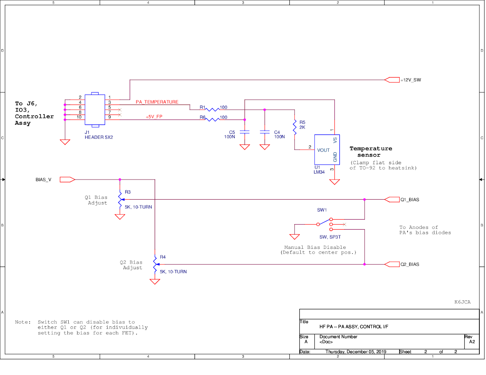
PA Control Circuit:
I added additional circuitry for control of the PA:

Notes on the Controller Interface schematic:
Some photos:
Printed-Circuit Assembly:

Temperature sensor clamped to copper heat-spreader:

Notes on the Build:
1. I used SMA connectors for both the PA input and its output. Using an SMA at the output may seem like a risk -- it is such a small connector! But I found the following information which states that, theoretically, an SMA should be good to at least 1000 watts at 100 MHz:

However, as the document states, this is theoretical.
Never the less, given typical SMA connector ratings of 350 to 500 Vrms, there would seem to be sufficient voltage margin for operation at, say, 600 watts into a load 1:1 SWR, in which the max voltage would be 173 Vrms. (Voltage, of course, could increase if the SWR increased).
I haven't found a spec for SMA current handling. Note that the current for 600 watts into 50 ohms would be about 3.5Arms. But this would be peak RMS current. Average current would be much less for SSB or CW operation.
If I assume an average power of 150 watts (i.e. an AM signal whose peak output power is 600 watts), the average current (into 50 ohms) would be 1.7 Amps. And besides, 150 watts average power is well below the kilowatt-plus rating in the chart, above.
So should it be OK? Fingers crossed! But so far no problem...
2. As for interconnecting coax cables on the RF Output side, RG400 (or equivalent) would seem to be a good choice -- one can purchase prefabricated cables with SMA connectors on either end, and I've seen specs for RG400 in which it is rated to 1900 watts at 30 MHz. Other specs state 2.7 KW at 30 MHz. Both of these specifications are well beyond my operating power, so the cable should be OK.
PA Performance Measurements:
IMD Summary:
(IMD measurements must be made with the Low-pass Filter in place)

80 Meter IMD:
80 Meter IMD Power-sweep:

80 Meter IMD at 505 Watts:

And 80 Meter IMD at 593 Watts -- although IMD3 is now slightly worse than -30 dBc, it's not too bad:

One question is -- is the IMD measured at the output a function of IMD at the amplifier's input. Here's a measure of IMD from the ENI 525LA Amplifier driving the PA during the power-sweep:

You can see that the input IMD3 is -41 dBc at the same point where the PA's output IMD3 is -31 dBc. So the input IMD3 is 10 dB better than the output IMD3.
Does this mean that there is no influence from the input IMD3? I can't say, but a 10 dB delta between input and output seems significant to me.
Never the less, it is a measurement-uncertainty to keep in mind.
40 Meter IMD:
40 Meter IMD Power-sweep:

40 Meter IMD at 487 Watts:

40 Meter IMD of the ENI 525LA Amplifier while driving the PA during the power-sweep:

Note that the output IMD3 at 487 watts out is -48.6 dBc, while the IMD3 of the driving signal for this output power is slightly worse (-44 dBc).
20 Meter IMD:
20 Meter IMD Power-sweep:

20 Meter IMD at 484 Watts:

20 Meter IMD of the ENI 525LA Amplifier while driving the PA during the power-sweep:

Note that, although the output IMD3 at 484 watts -31.4 dBc, the input IMD3 is -48 dBc.
17 Meter IMD:
17 Meter IMD Power-sweep:

17 Meter IMD at 505 Watts:

17 Meter IMD of the ENI 525LA Amplifier while driving the PA during the power-sweep:

Note that, at 505 watts out, the output IMD3 is -34.8 dBc while the input IMD3 is -44.7 dBc.
15 Meter IMD:
15 Meter IMD Power-sweep:

15 Meter IMD at 494 Watts:

15 Meter IMD of the ENI 525LA Amplifier while driving the PA during the power-sweep:

At 494 watts out, the output IMD3 is -39.8 dBc, while the input IMD3 is -47.3 dBc.
12 Meter IMD:
12 Meter IMD Power-sweep:

12 Meter IMD at 499 Watts:

12 Meter IMD of the ENI 525LA Amplifier while driving the PA during the power-sweep:

At 499 watts out, the output IMD3 is -34.5 dBc, while the input IMD3 is -47.4 dBc.
10 Meter IMD:
10 Meter IMD Power-sweep:

10 Meter IMD at 500 Watts:

10 Meter IMD of the ENI 525LA Amplifier while driving the PA during the power-sweep:

At 500 watts out, the output IMD3 is -31.2 dBc, while the input IMD3 is -46.6 dBc.
Gp (Power Gain) versus Power Out, by Band:
Here's a plot of the amplifier's "power gain". (See the important note just below it!)

An Important Note regarding my calculation of Gp!
I've calculated Gp as the ratio of Power-Out (into a 50 ohm load) from the PA, divided by Forward-powered (measured using a directional coupler) into the PA.
But Gp is actually the ratio of Power-Out divided by the power delivered to the PA. Forward-power is not the same as power-delivered.
Forward-power is actually the power-delivered to the load plus the power reflected from that load. So, the power actually delivered to the PA should be the difference between Forward-power and Reflected-power.
For example, if Forward power at the PA's input were 10 watts and the Reflected power were 2.5 watts (i.e. an SWR of 3:1), only 7.5 watts is actually delivered to the PA, and thus Gp should be calculated using this 7.5 watts, not the 10 watts.
But measuring both Forward-power and Reflected-power gets to be time-consuming (for my test setup). Fortunately, in the case of this PA in which the input SWR is on the order of 1.5:1 or so, we can use Forward-power as a close approximation to the power that is actually delivered to the PA.
Here's an example:
Let's assume the SWR at the PA input is 1.58:1. This corresponds to a system in which the reflected-power is 5 percent of the forward-power (i.e. if forward-power were 100 watts, reflected-power would be 5 watts, and power-delivered would be 95 watts).
That is, the power actually delivered to the input of the PA would be 0.22 dB less than the Forward-Power measurement at the PA's input.
So, in this case of an input SWR of 1.58:1, the actual Gp should be about 0.22 dB greater than the Gp calculated using Gp = Pout / (Input_Pfwd).
And thus, for this PA (where the measured power gain is at least 12 dB), the Gp error is less than 2%.
In other words, for this PA, the Gp error is insignificant.
Input SWR and Efficiency at 500 Watts (approximately), by Band:

Efficiency versus Power Out, 80 meters:

(For measurements of this amplifier's Harmonic Distortion: please refer to the Low-pass Filter blog post.)
Testing Methodologies:
IMD Testing:
I measure IMD using the following test setup:
 The ENI 525LA is a linear amplifier providing 50 dB of gain at outputs
up to 25 watts (but distortion increases quickly at high power).
The ENI 525LA is a linear amplifier providing 50 dB of gain at outputs
up to 25 watts (but distortion increases quickly at high power).
The other items should be self-explanatory. Note that the test system is controlled via GPIB using a Matlab script written by Dick Benson, W1QG. Here's a photo of the GPIB devices and the laptop I used to control them.

Some notes on the IMD Test System:
1. The E4406A's internal attenuator is set to 30 dB. (Internal attenuation is required with an 8568B Spectrum Analyzer when making IMD measurements to keep its internal distortion from mucking with the results, and I've continued this practice with the E4406A, whether it needs it or not.)
2. The HP 3335A generator outputs are coupled to each other via a Mini-Circuits ZSC-2-1 Power Splitter/Combiner, which does not provide much isolation between the outputs. Fortunately, each HP 3335A generator output level seems to be immune from the influence of the other HP 3335A's output, as you can see in the image, below:

(Please refer to the note-box in the screen-capture for a description of the test setup).
Prior to my creating the two-tone signal with two 3335A generators, I tried using a 3335A with an HP 8643A. The result was not so good:

My theory is that the 8643A's output stage is susceptible to external signals (perhaps via an ALC loop)? Fortunately, I was able to pick up a second HP 3335A on eBay.
A note on ENI 525LA Distortion:
The ENI 525LA amplifier that I use to amplify the two-tone signal created with the two HP 3335A generators can create its own IMD distortion that worsens at high power.
- Change T2 Feedback winding from 3 turns to 7 turns.
- Remove C3 and Replace R3 with a short.
- Remove C4 and Replace R4 with a short.
- Cut the trace going from R8 to the C2, C6, T1 group of components.
- Cut the trace going from R12 to the C2, C7, T1 group of components.
- Jumper the now-floating pin of R8 to the Gate of Q1 using a leaded 0.1, 100V ceramic cap.
- Jumper the now-floating pin of R12 to the Gate of Q2 using a leaded 0.1, 100V ceramic cap.
PA Control Circuit:
I added additional circuitry for control of the PA:
Notes on the Controller Interface schematic:
- The +12V_SW power (from the Controller assembly, via connector J1) is switched on/off by the Controller, thus allowing bias to be removed from the PA during Receive or if a fault occurs during transmit.
- R3 and R4 are now 10-turn pots (to allow me to more easily adjust for equal bias currents in the two FETs).
- I added switch SW1 (three position toggle) to allow me to disable one FET or the other, which lets me easily check if their bias currents are equal. For normal operation, this switch is set to its "center" position so that neither FET gate is grounded.
- R1/C4 and R6/C5 are some simple 1-pole filters to knock down any external RF that might be coming in via the wiring.
- The 2K resistor, R5, is recommend by TI's LM34 datasheet (figure 12) if the output is heavily capacitive loaded. I don't know what the capacitive loading actually is, but I decided it wouldn't hurt to include the resistor and it might even be a benifit.
Some photos:
Printed-Circuit Assembly:

Temperature sensor clamped to copper heat-spreader:

Notes on the Build:
1. I used SMA connectors for both the PA input and its output. Using an SMA at the output may seem like a risk -- it is such a small connector! But I found the following information which states that, theoretically, an SMA should be good to at least 1000 watts at 100 MHz:

However, as the document states, this is theoretical.
Never the less, given typical SMA connector ratings of 350 to 500 Vrms, there would seem to be sufficient voltage margin for operation at, say, 600 watts into a load 1:1 SWR, in which the max voltage would be 173 Vrms. (Voltage, of course, could increase if the SWR increased).
I haven't found a spec for SMA current handling. Note that the current for 600 watts into 50 ohms would be about 3.5Arms. But this would be peak RMS current. Average current would be much less for SSB or CW operation.
If I assume an average power of 150 watts (i.e. an AM signal whose peak output power is 600 watts), the average current (into 50 ohms) would be 1.7 Amps. And besides, 150 watts average power is well below the kilowatt-plus rating in the chart, above.
So should it be OK? Fingers crossed! But so far no problem...
2. As for interconnecting coax cables on the RF Output side, RG400 (or equivalent) would seem to be a good choice -- one can purchase prefabricated cables with SMA connectors on either end, and I've seen specs for RG400 in which it is rated to 1900 watts at 30 MHz. Other specs state 2.7 KW at 30 MHz. Both of these specifications are well beyond my operating power, so the cable should be OK.
PA Performance Measurements:
IMD Summary:
(IMD measurements must be made with the Low-pass Filter in place)

80 Meter IMD:
80 Meter IMD Power-sweep:

80 Meter IMD at 505 Watts:

And 80 Meter IMD at 593 Watts -- although IMD3 is now slightly worse than -30 dBc, it's not too bad:

One question is -- is the IMD measured at the output a function of IMD at the amplifier's input. Here's a measure of IMD from the ENI 525LA Amplifier driving the PA during the power-sweep:

You can see that the input IMD3 is -41 dBc at the same point where the PA's output IMD3 is -31 dBc. So the input IMD3 is 10 dB better than the output IMD3.
Does this mean that there is no influence from the input IMD3? I can't say, but a 10 dB delta between input and output seems significant to me.
Never the less, it is a measurement-uncertainty to keep in mind.
40 Meter IMD:
40 Meter IMD Power-sweep:

40 Meter IMD at 487 Watts:

40 Meter IMD of the ENI 525LA Amplifier while driving the PA during the power-sweep:

Note that the output IMD3 at 487 watts out is -48.6 dBc, while the IMD3 of the driving signal for this output power is slightly worse (-44 dBc).
20 Meter IMD:
20 Meter IMD Power-sweep:

20 Meter IMD at 484 Watts:

20 Meter IMD of the ENI 525LA Amplifier while driving the PA during the power-sweep:

Note that, although the output IMD3 at 484 watts -31.4 dBc, the input IMD3 is -48 dBc.
17 Meter IMD:
17 Meter IMD Power-sweep:

17 Meter IMD at 505 Watts:

17 Meter IMD of the ENI 525LA Amplifier while driving the PA during the power-sweep:

Note that, at 505 watts out, the output IMD3 is -34.8 dBc while the input IMD3 is -44.7 dBc.
15 Meter IMD:
15 Meter IMD Power-sweep:

15 Meter IMD at 494 Watts:

15 Meter IMD of the ENI 525LA Amplifier while driving the PA during the power-sweep:

At 494 watts out, the output IMD3 is -39.8 dBc, while the input IMD3 is -47.3 dBc.
12 Meter IMD:
12 Meter IMD Power-sweep:

12 Meter IMD at 499 Watts:

12 Meter IMD of the ENI 525LA Amplifier while driving the PA during the power-sweep:

At 499 watts out, the output IMD3 is -34.5 dBc, while the input IMD3 is -47.4 dBc.
10 Meter IMD:
10 Meter IMD Power-sweep:

10 Meter IMD at 500 Watts:

10 Meter IMD of the ENI 525LA Amplifier while driving the PA during the power-sweep:

At 500 watts out, the output IMD3 is -31.2 dBc, while the input IMD3 is -46.6 dBc.
Gp (Power Gain) versus Power Out, by Band:
Here's a plot of the amplifier's "power gain". (See the important note just below it!)

An Important Note regarding my calculation of Gp!
I've calculated Gp as the ratio of Power-Out (into a 50 ohm load) from the PA, divided by Forward-powered (measured using a directional coupler) into the PA.
But Gp is actually the ratio of Power-Out divided by the power delivered to the PA. Forward-power is not the same as power-delivered.
Forward-power is actually the power-delivered to the load plus the power reflected from that load. So, the power actually delivered to the PA should be the difference between Forward-power and Reflected-power.
For example, if Forward power at the PA's input were 10 watts and the Reflected power were 2.5 watts (i.e. an SWR of 3:1), only 7.5 watts is actually delivered to the PA, and thus Gp should be calculated using this 7.5 watts, not the 10 watts.
But measuring both Forward-power and Reflected-power gets to be time-consuming (for my test setup). Fortunately, in the case of this PA in which the input SWR is on the order of 1.5:1 or so, we can use Forward-power as a close approximation to the power that is actually delivered to the PA.
Here's an example:
Let's assume the SWR at the PA input is 1.58:1. This corresponds to a system in which the reflected-power is 5 percent of the forward-power (i.e. if forward-power were 100 watts, reflected-power would be 5 watts, and power-delivered would be 95 watts).
That is, the power actually delivered to the input of the PA would be 0.22 dB less than the Forward-Power measurement at the PA's input.
So, in this case of an input SWR of 1.58:1, the actual Gp should be about 0.22 dB greater than the Gp calculated using Gp = Pout / (Input_Pfwd).
And thus, for this PA (where the measured power gain is at least 12 dB), the Gp error is less than 2%.
In other words, for this PA, the Gp error is insignificant.
Input SWR and Efficiency at 500 Watts (approximately), by Band:

Efficiency versus Power Out, 80 meters:

(For measurements of this amplifier's Harmonic Distortion: please refer to the Low-pass Filter blog post.)
Testing Methodologies:
IMD Testing:
I measure IMD using the following test setup:

The other items should be self-explanatory. Note that the test system is controlled via GPIB using a Matlab script written by Dick Benson, W1QG. Here's a photo of the GPIB devices and the laptop I used to control them.

Some notes on the IMD Test System:
1. The E4406A's internal attenuator is set to 30 dB. (Internal attenuation is required with an 8568B Spectrum Analyzer when making IMD measurements to keep its internal distortion from mucking with the results, and I've continued this practice with the E4406A, whether it needs it or not.)
2. The HP 3335A generator outputs are coupled to each other via a Mini-Circuits ZSC-2-1 Power Splitter/Combiner, which does not provide much isolation between the outputs. Fortunately, each HP 3335A generator output level seems to be immune from the influence of the other HP 3335A's output, as you can see in the image, below:

(Please refer to the note-box in the screen-capture for a description of the test setup).
Prior to my creating the two-tone signal with two 3335A generators, I tried using a 3335A with an HP 8643A. The result was not so good:

My theory is that the 8643A's output stage is susceptible to external signals (perhaps via an ALC loop)? Fortunately, I was able to pick up a second HP 3335A on eBay.
A note on ENI 525LA Distortion:
The ENI 525LA amplifier that I use to amplify the two-tone signal created with the two HP 3335A generators can create its own IMD distortion that worsens at high power.
This additional IMD coming in through the PA's input will cause Uncertainty in the PA's measured IMD performance at its output.
I discuss this issue further in the following blog-post: IMD Uncertainty due to Source Distortion. Below are IMD plots with "worst-case" values calculated using the technique described in that blog-post.


Input SWR Testing:
To test the input SWR I simply drive the PA to full power out and measure its input SWR with an LP-100 power meter.

Power Gain Testing:
As I mentioned above, I calculate power-gain using a forward-power measurement made at the input of the Power Amplifier during the IMD power-sweep.
I measure the input forward-power with my "home-brew" directional coupler. This directional coupler has a coupling factor of -24 dB. To prevent overdriving the HP 4406A Spectrum Analyzer's input, I add an additional 23 dB of attenuation (for a total loss of 47 dB) between the directional coupler's "FWD" port and the E4406A's input.
Here's the setup. To change between output IMD and input IMD measuring, I simply swap which source drives the E4406A's input cable (i.e. the 50 dB Output Attenuator's output or the input directional coupler plus attenuator's output), making sure that I terminate the other now-unconnected output with 50 ohms.

For a discussion on limitations of Agilent's E4406A, see my notes, further below.
Heat Sink Notes:
I'm not sure where I found this "junkbox" heatsink -- but it was originally too large for this application, and so I cut it down to size:


On top of this I placed a copper plate to act as a heat-spreader. The copper-plate is slightly larger in surface area than the heat-sink and thus overlaps it. It is slightly less than a quarter-inch thick.
I spread a thin layer of heatsink compound (Boron Nitride Heat Sink Grease) between the copper heat-spreader and the heatsink as well as between the heat-spreader and components that attach directly to it (e.g. the VRF2944 FETs, etc.). It seems to work well enough.
Other Notes:
1. Note from Frank Carcia, WA1GFZ:
After I published this post Frank Carcia (WA1GFZ) sent me the following note. Frank is the author of the article "High Power Solid Stated Broadband Linear Amplifiers, a Different Approach," which appeared in the Sept/Oct 2015 issue of QEX (and referenced by Dick Frey earlier in this post).
Jeff,
I simulated a number of different output transformer
configurations. Your configuration I found the shunt DC feed
choke reactance effected the broadband performance. The
inductance of the choke would shift the response. I couldn't
find a value that would work from 160m to 6m. The performance
started to fall apart around 15 meters with too much inductance
or 80/160m with too small inductance.
Then I simulated the Amplifier Research output configuration.
This configuration removes your shunt feed choke and feeds DC
directly into the common shield connection where the two
transformer primaries meet. This configuration worked very well
as long as you ran class A. Once you reduce the bias the IMD was
nasty. AR runs their BB amps in class A.
Last I ran my configuration with both transformer phases on a
common core. This allowed for less turns (Jerry Servick
observation). The advantage is you get the balancing effect of
the shunt feed without adding drain reactance and less wire to
help with broadband operation. The bias level is still sensitive
as you observed due to the FET transfer curve but far better
than the Amplifier Research configuration.
I also simulated the typical flux transformer dc into the
center tap configuration. That works but the wire lengths of the
secondary add up leakage inductance limiting BB operation.
The best transformer I built was using 1 type 43 balun core
like you have with 1 turn through both holes for each
phase.
I had to stand them on end to make the connections and put
sharp bends in the cable in order to solder them to the PC
board.
This only used 5 1/2 inches of cable for each phase. The
performance was great and I bet would cover 2 meters but I was
afraid the cables with sharp turns would Teflon flow in time and
I had no way to support the cores. My case the ferrite sleeve
was easier to deal with but I had to go to two turns per phase
increasing the cable length to about 11 inches per
phase.
That didn't hurt my efficiency on 6 meters but I don't think 2
meters would work. I could have used type 61 and proved it with
testing stacks of toroids. I even tried type 67 which is even
lower loss using 3 turns per phase. The flux density is so low
on 6 meters that the type 43 worked fine.
My driver amplifier I found a type 43 sleeve slightly bigger
that allowed me to get away with 1 turn per phase and still have
enough inductance for 160m. This was the best of both worlds and
would have allowed me the shorter cable length maybe even
shorter than the balun core.
I was all set to go to that size until I checked the price of
the core. It is not a popular size and the price was a lot
higher. I dropped that idea when my 6 meter performance
matched the rest of the bands.
So if you want a bit more mental torture get your amp to cover
6 meters...
I can run 1 KW carrier on AM on 6 meters but when I checked the
field strength I found it was a bit unsafe. I stick to around
200 watts so I don't do any damage. The tower is only 20 feet
from the house.
gfz
Dick Benson, W1QG, first informed me of the capabilities of the Agilent E4406A Vector Signal Analyzer "Transmitter Tester", and he has developed some MATLAB code for communicating with the tester via GPIB and analyzing its data.
The text below is from Dick's document describing his MATLAB code and the E4406A (found here -- but please note, his MATLAB package does not contain the code for doing sweeps of IMD and Gain versus Power that I used, above.)
Per Dick...
Some of the E4406A limitations are:
1) Its maximum "Span" is 10 MHz. This limits its utility as a general purpose Spectrum Analyzer.
2) Its first IF is 321.4 MHz, and the is no filtering before the first mixer. This means that images are very likely, and these can lead to confusion. For example, if the analyzer's center frequency is set to 50 MHz, the first LO will be set to 50+321.4 = 371.4 MHz. A signal fed into the analyzer at 692.8 MHz will produce an identical 321.4 MHz output from the first mixer since 692.8-371.4 = 321.4 MHz.
3) The input frequency range specs have a "hole": 7 to 314 MHz and 329 MHz to 4 GHz
4) There is no "Trace Memory" to allow A vs B measurement comparisons. Virtually all of these annoyances are addressed by the vsa_gui_1.m application.
Workarounds to the Limitations:
1) The 10 MHz maximum Span is addressed by stitching together multiple 10 MHz (or less) "chunks" of spectrum to cover a "Span" that is greater than the instrument's 10 MHz limit. This works remarkably well. But keep in mind that where the E4406a truly excels is in making narrow band measurements.
2) The mixer image problem can be addressed by using an external filter to limit the input signal frequency content to a known region. For instance, I use a 160 MHz low pass filter most of the time since my interests usually lie in the 3 to 160 MHz region.
3) It has been found that the analyzer works quite well down to about 1.5 MHz. Below this, the amplitude accuracy and linearity of the front end start to degrade. As to the hole between 314 and 329 MHz, well, just avoid it! However, you will find that most of this range is actually usable for narrow band analysis. Clearly an input signal at or very near 321.4 MHz should be avoided due to the first mixer RF-to-IF feed through.
4) Implementing "Trace Memory" is easy in MATLAB, and an invaluable feature.
That's it for this post. Continue on to the other posts in this series via the links, below...
K6JCA HF PA Posts:
- A 500 Watt HF PA, Part 1: Overview
- A 500 Watt HF PA, Part 2: PA (and Bias) Assembly
- A 500 Watt HF PA, Part 3: Low-pass Filter Assembly (including LPF-Input Directional Coupler)
- A 500 Watt HF PA, Part 4: Power Supply and Supervisory Circuitry
- A 500 Watt HF PA, Part 5: T/R Switching and Output Directional Coupler
- A 500 Watt HF PA, Part 6: Front Panel and Controller Assembly
- A 500 Watt HF PA, Part 7: Back Panel, Interconnects, and Miscellaneous
- A 500 Watt HF PA, Part 8: Complete Schematics
Standard Caveat:
I might have made a mistake in my designs, schematics, equations, models, etc. If anything looks confusing or wrong to you, please feel free to leave a comment or send me an email.
Also, I will note:
This design and any associated information is distributed in the hope that it will be useful, but WITHOUT ANY WARRANTY; without an implied warranty of MERCHANTABILITY or FITNESS FOR A PARTICULAR PURPOSE.


1 comment:
Very clear and clean.
Many hours sent to reach the target but very nice amplifier.
Best 73
Gérard / F6EHJ
Post a Comment