Saturday, May 23, 2020

ME-165/G Standing Wave Ratio - Power Meter


The ME-165/G is a military SWR and Power meter, designed for the HF bands (1.5 - 30 MHz), that includes an internal 600 watt dummy load.

The image, below, shows the ME-165/G as part of the AN/GRC-26D shelter-mounted radio teletype station:


The unit provides a convenient way to switch the dummy load in and out of the transmission line, plus, if tuning an antenna tuner in SWR mode, its SWR circuitry allows the transmitter to always see a 50 ohm load, irrespective of the actual load at the unit's Output port.  So you don't need to worry about destroying your finals if you make a mistake while tuning your antenna tuner.

There are four modes of operation (per the four positions of the front panel's rotary switch).  The table below describes how the ports connect and the meter function for each of these four modes:


The following illustration shows this same information as a "functional diagram" (i.e. part block diagram, part schematic).


Antenna Tuning Procedure:

When tuning an antenna tuner, the ME-165/G should first be placed into "ADJUST" mode and the "ADJUST" potentiometer rotated for a full-scale meter reading while transmitting a CW signal.

Then turn the rotary switch to its "SWR" position and adjust an external antenna tuner (connected between the ME165/G's Output connector and the antenna) to give a minimum reading on the SWR meter (for a correctly tuned tuner, the meter's needle should end up in the green-region at the left-hand side of the scale).

Here is a closeup of the Power and SWR meter scales:


Note that the SWR scale is NOT accurate above about 2:1.  (I'll discuss this in more detail later in this blog post).


Schematic:

The schematic, from the Army's Technical Manual.  I've corrected a couple of errors (my corrections are in red):


Also, note that C8 (the capacitor at the Input connector) is listed in the schematic as 40 pF.  In the two ME-165/G units that I have, its capacitance is actually 39 pF.

Schematic Notes:

1.  The 1200 ohm, 25 watt resistor, R15 in the schematic, in series with the SWR Bridge circuit reduces the power delivered to the SWR bridge circuit (therefore, the bridge can use 1/2 watt resistors).

2.  SWR Detection is via a Wheatstone bridge.  The bridge is balanced when the load at the ME-165/G's Output port is 51 ohms.

3.  C6 puts the ADJUST pot wiper at RF Ground, thus R22 (1200 ohm) is essentially in parallel with the  lower-right-hand side side of the bridge (via C5) -- i.e. this resistance is in parallel with whatever load is attached to the unit's Output port.

Thus, an equivalent resistance (R20, 1200 ohms) must be connected in parallel with the lower-left-hand arm of the bridge to ensure that the bridge is balanced when the external antenna impedance connected at the Output side of the bridge is 51 ohms, resistive.


ME-165/G Performance:

I own three ME-165/G's.  Let's look at their performance.

First, the unit manufactured by Radalab, Inc:

The (first) Radalab, Inc., ME-165/G (circa 1970's):

I picked up this unit many years ago.  The unit was in good shape, but a previous owner had replaced the original N connectors with SO-239 connectors.


Inside, the majority of the components are wired point-to-point using solder posts:


Below is a photo showing the wiring from one side of the Dummy Load to the rotary switch and from the other side of the Dummy Load to ground.  Note that the load's ground wire goes to C8's ground terminal.  This terminal is then grounded to the front panel via a separate wire.

The other wire from the load (to the rotary switch) is bound tightly with the ground wire from the load, using three cable ties.


The 50 ohm, 600 watt load consists of twelve Dale 600 ohm, 50 watt resistors in parallel:


S-Parameters:

Measuring the unit's S-Parameters in dummy-load mode with an HP 8753C Network Analyzer:


Below is the capture of S11 when the ME-165/G's rotary switch is set to POWER (i.e. the Input port is connected to the 50 ohm Dummy Load).  You can see that the SWR in the HF band (to 30 MHz) looks very good (1.1:1 at 30 MHz).  Not so good at 6 meters, but this load is not spec'd to that frequency.


When the front-panel rotary switch is in the OPERATE position, the dummy load is disconnected from the Input connector and the Input is connected directly to the Output connector.

How does the Radalab ME-165/G affect performance when it is in its OPERATE mode?  Again, let's look at the s-parameter measurements...

As you can see in the plot below, there is some insertion loss that worsens with frequency, but this loss is only about 0.09 dB, worst case, at 30 MHz.


And the SWR of the "ideal" 50 ohm external load, rather than being 1:1, is now changed by the Radalab ME-165/G to be 1.2:1 (at 30 MHz).


So, some minor adverse effects, but overall, not bad!

Improving the performance of this (first) Radalab ME-165/G in OPERATE mode:

I had noticed a difference between the Oneida's output wiring and the wiring of the Radalab unit, and I wondered if this difference accounted for the slightly worse Radalab Insertion Loss when in OPERATE mode.

The wiring from the rotary switch to the Oneida unit's output connector had been routed next to the front panel.  But the same wire in the Radalab unit was routed high in the air, as shown below:


Would moving this output wire to be closer to the front panel make a difference?  Here's a photo of the new routing:


And below is the measured s-parameters for this new routing.  Note that Insertion loss has decreased from 0.09 dB to about 0.07 dB.  Note much of a change, but it's in the right direction.


And the image below shows that the SWR of the "ideal" 50 ohm load is now 1.1:1 (from 1.2:1).  Again, a slight improvement, but an improvement never-the-less.


Oneida Electronics Inc ME-165/G (circa 1963):

My second ME-165/G was manufactured by Oneida Electronics Inc, around 1963 (per the suffix on the Order Number listed on the front panel tag).

This unit still has the stock N-connectors on the front panel (note that in the image, below, there are BNC adapters attached).


Here's a look at the inside terminal-board used for wiring the components.  You can see that it is similar to the later Radalab's board (shown above):


But there is one noticeable difference between the Radalab board and the Oneida board, which is the use of clips to hold in CR1 and CR2, rather than soldering them to posts, as shown in the two photos, below:

CR1 (1N69A)


CR2 (1N277)


I imagine clips allowed easy replacement of the original 1N69A diodes in case they blew out.  Note that CR2 (a 1N277 diode) has its leads wrapped around the clip's posts.  This diode probably replaced a bad 1N69A diode.

The image below shows Oneida's wiring from the 600 watt dummy load to the rotary switch and ground.  Note the difference between this wiring and the wiring in my Radalab unit (shown earlier in this post).  The wires below are not routed together in parallel, and the dummy load's ground wire goes directly to a ground terminal on the front panel, rather than first routing to C8's ground.


Also, the dummy load's resistors are not Dale resistors; instead they are TRU-OHM 600 ohm non-inductive resistors:


Improving the performance of the Oneida ME-165/G:

When I first measured the SWR of the dummy load, I noticed that it rose to 1.5:1 at 30 MHz.  So I tried to improve its SWR by changing the dummy load's wiring to look exactly like the wiring in my Radalab   ME-165/G.

But with this modification the SWR rose to 1.75:1 at 30 MHz (see below).  Yikes -- my attempt to make the Oneida's wiring match the Radalab wiring moved SWR in the wrong direction!


OK -- mimicking the Radalab's wiring was not going to work.  Playing around with the separation of the dummy load's two wires, I discovered that (a) separating the two wires far apart, and (b) keeping the     original ground wire to the dummy load, in addition to the new (red) ground wire I'd added, improved the SWR.

The image below shows the new dummy-load wiring.  The red wires are 14 AWG THHN stranded wires (insulation rated to 600V).  Note their separation! You can see the dummy load's grounding red wire goes to C8, just like the wiring in the Radalab unit.  But you can also see that the original ground wire is still connected to the dummy load (and now routed a bit closer to the upright mounting plate).


And here is the new SWR measurement.  Now it is 1.2:1 at 30 MHz.


(Perhaps the difference in wiring is due to a difference in impedance between the Oneida's 600 ohm TRU-OHM resistors and the Dale 600 ohm resistors in the Radalab unit?)

In OPERATE mode the Oneida unit's measurements look very good.  Here's S21.  Insertion loss is only about 0.04 dB at 30 MHz.


And there is little impact on the SWR of an external 50 ohm load.  As you can see, below, the SWR at 30 MHz for the external 50 ohm load is 1.09:1.


Second Radalab, Inc., ME-165/G (S/N 47C):

The first Radalab unit I discussed (above) is serial number 7C.  This second ME-165/G is serial number 47C.

Interestingly, its component-mounting board no longer has the clips for the diode leads.  Instead, all components are attached with soldering posts:


(This difference could be due to a later unit upgrade, or it might have been a change during the manufacturing run).

Otherwise, the two Radalab units look very similar.

S-Parameters:

Again, made with my HP 8753C Vector Network Analyzer.

Below is the S11 plot with the Function Switch set to POWER.  Note that the SWR at 30 MHz is about 1.5:1.  Not as good as I would like it to be.


Below are the s-parameters with the Function Switch set to OPERATE:


SWR (of an external 50 ohm load) is transformed to about 1.3:1 (from the load's original 1:1) at 30 MHz.

And Insertion Loss is about 0.1 dB.

Improving the performance of this second Radalab ME-165/G:

The image below shows the original wiring of this ME-165/G:


If I routed the dummy-load wires together (using tie-wraps), SWR in POWER mode improved.

The image below shows the new routing of the two dummy-load wires:


(Note, I had to trim off a small amount of the wire going to the big black cap because it was just a too long, as you can see in the photo, below.)


With this modification, the dummy-load's SWR went from 1.5:1 to less than 1.1:1 (see below).


I had noted that the wire to the output jack was up in the air.  So I moved it to route along the inside of the front panel.

I don't know the voltage rating of this wire's insulation, and I was a concerned that it now ran against the grounded metal of the front panel, so to prevent the possibility of arcing I added a bit of Kapton tape between it and the panel for extra voltage insulation (and I added a second piece of tape to hold the wire next to the panel), as shown below:


This modification improved OPERATE mode's Insertion Loss (from 0.1 dB to about 0.05 dB) and the "through" SWR of an external 50 ohm load (now 1.1:1 from the unmodified version's 1.3:1).


An SWR Meter that does not measure SWR:

While using the ME-165/G,  I discovered that its SWR readings can be very inaccurate'

Here's a look at the SWR scale on the ME-165/G meter.


As I mentioned, the SWR reading can sometimes by quite inaccurate.  For example, what should be the SWR when the load is a short?  Of course, it should be infinite (meter needle at full scale).  But that's not what the ME-165/G shows:


So my Radalab unit shows that the SWR of a short-circuit is somewhere between 3:1 and 4:1.  And if I repeat the test on my Oneida unit, the SWR of a short measures slightly less than 3:1 (the difference between the two is probably due to drift of component values over time).

In other words, both of my ME165/G SWR meters show an SWR of around 3:1 for a short circuit.  Neither unit shows the correct SWR of infinity (meter needle at full scale).

Despite this gross SWR inaccuracy for a short-circuit load, the SWR meter's accuracy seems to improve considerably below an SWR of about 2:1.  Therefore, as long as the goal is to tune the antenna for minimum SWR, rather than measure its SWR value, the ME-165/G does the job quite well.

But I still wanted to know -- why was the SWR meter so inaccurate for a short-circuit load?


SPICE Simulations:

I decided to do some SPICE simulations to get a better understanding of what to expect from the ME-165/G SWR detector.

The ME-165/G's SWR measurement circuit is based upon a simple Wheatstone Bridge, with the unknown load to be measured represented by the lower right-hand arm of the bridge, as shown, below:
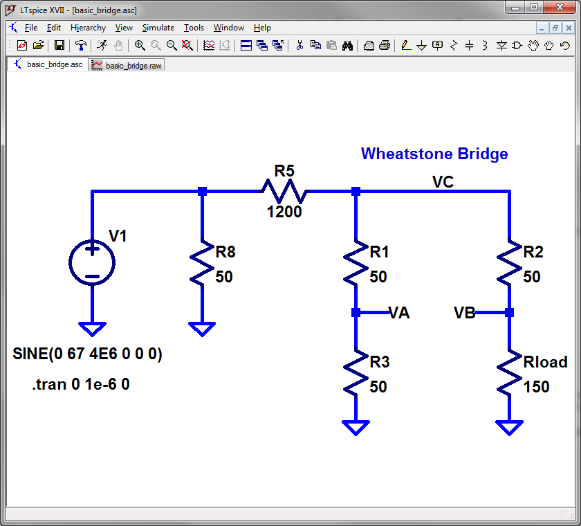

In an ideal Wheatstone Bridge we can take the difference between Va and Vb, then divide by Va, and then take the magnitude of this value, we can create a set of numbers that we can equate to SWR values, as shown in the table, below:


Note that the quantity |(Va - Vb)/Va| is equivalent to the magnitude of the load's Gamma:

|Γ|    SWR
    0     1.00 
 0.1     1.22
 0.2     1.50
 0.3     1.86
 0.4     2.33
 0.5     3.00
 0.6     4.00
 0.7     5.67
 0.8     9.00
 0.9   10.00
 1.0   infinite


In other words, if we could measure Va and Vb with high impedance measuring circuits (so that there are no unwanted currents through either arm of the bridge that might alter the bridge's balance) and then perform the math, we'd get a number equal to the magnitude of the load's Gamma, and thus translatable to its SWR.

Sounds straightforward, but note...the equation requires a division by Va.  Is there an easy way to accomplish this division with simple circuitry?

If we could adjust our voltages so that Va equals 1 (while keeping the ratio of Va to Vb constant), then we can skip the division step, because we would be dividing by 1.

In the bridge circuit above, for example, maybe we would have a switch that we would first set to an "Adjust" position, connecting a high-impedance meter to Va and letting us scale its gain (via a potentiometer) until the meter's needle is at Full Scale, i.e. so that Va now equals 1.

And then we would flip the switch to measure |Va - Vb|, using the same gain-adjusted high-impedance meter, to give us a direct reading of  Gamma thus SWR (e.g. a meter reading of 1/2 Full Scale would equal a Gamma of 0.5, or an SWR of 3:1).

But we can see from the SWR scale on the ME-165/G meter, and from our example measuring the SWR of a 0 ohm load, that the ME-165/G is doing something very different -- something that affects the accuracy of its SWR readings.

The problem is that, for the equation Vswr = |(Va-Vb)/Va| to give accurate results, Va must be measured while Rload is connected to the Wheatstone Bridge. This is because, given the ME-165's circuitry to limit the power to the Wheatstone Bridge (i.e. the series 1200 ohm, 25 watt resistor ), any change in Rload will affect the voltage at node Vc at the top of the bridge (because a change in Rload will change the current through that arm of the bridge, and thus it changes the current (and subsequent voltage drop) through this series 1200 ohm resistor feeding the bridge).

Because we are adjusting Va to be 1 (to avoid a mathematical division), the value of Va that was set during the "Adjust" step should (ideally) be the same as the value of Va used during the SWR measurement step.

But in the ME-165/G, these two Va's are not the same.  The Va of the Adjust step is measured without Rload connected to the bridge, while Va of the SWR measurement step is measured with Rload connected to the bridge.

So Vc will be different for these two steps, and thus Va (which equals Vc/2) will also be different.

Let Va1 be the value of Va measured during the Adjust, and "Va2" be the value of Va measured during the SWR measurement step.  Because the "Adjust" step is, essentially, determining the value of Va that we will use to normalize the quantity (Va2 - Vb), the original equation  |(Va - Vb)/Va| becomes:

Vswr = | (Va2 - Vb) / Va1 |

I can simulate the result in LTSpice by adding another arm to represent the "unloaded" Va (i.e. Va1).  Below is the model, and I've annotated it with the simulation results of this new equation.


We can see that the measured SWR values are different for loads with the same actual SWR (e.g. 0.34 for 150 ohms versus 0.21 16.67 ohms -- both loads have an actual SWR of 3:1), and it explains why the ME165/G's measured SWR of a short is so far off from what it should be.


Let's now add the diode detector and meter circuit to the simulation and see how they affect performance.  Please note:

1.  LTSpice doesn't seem to have any Germanium diode models, so I'm using a Schottky diode (1N5817), instead.  (Note:  if replacing the original CR1 or CR2, I'd recommend using a 1N5818 or 1N5819 for their higher peak-reverse-voltage specifications.)
2.  I've adjusted the amplitude of the driving voltage source so that R23 (representing the "Adjust" potentiometer) is 0 ohms and the meter current is 1.0 mA when Rload = 1 Megohm (by setting the current equal to 1 mA for Rload = 1 Meg, I am effectively mimicking the "Adjust" step of the SWR measurement).
3.  The 1 mA meter is represented by Rmeter (58 ohms), per my measurement of the meter's resistance.  And I've increased the meter's bypass cap (C7) from 1 nF to 100 nF to knock down the RF across the meter and make it easier to determine the DC current passing through Rmeter.
4.  The frequency of the sine-wave drive is 4 MHz.
5.  Circuit parasitic elements are not included in the simulation.

I would expect the addition of the diode-detector to throw off the simulated values determined earlier (for the "ideal" Wheatstone Bridge), because the diode will conduct during part of the RF cycle, squirting current from the right arm of the Wheatstone Bridge (Vb) into the left arm (Va) and thus changing these two voltages.

Here's the new LTSpice schematic:


And below are some simulations of this new circuit...

First, verifying that the "meter" current is 1 mA when mimicking the ME-165/G in ADJUST mode, i.e. when there is no load (Rload = 1 Megohm):


Next, replacing the "open" load with a short.  Ideally, the current should remain 1 mA (representing an infinite SWR).  But as you can see, the DC current is 0.4 amps, which is quite a ways off from the 1 mA target.


Let's take a look at two loads that should each have an SWR of 3:1:

First, a Load = 150 ohms (note that the meter current is 0.32 mA):


Next, a Load = 16.67 ohms (note that the meter current is 0.21 mA):


These results are not exactly the same as the results made without the actual diode-detector in the circuit, but they are close.  (I believe the difference is due to the actual diode-detector acting as a current path between the two arms of the bridge, when in fact these two arms should be isolated from each other).

Below is a table of simulation results, simulated at 4 MHz and at 10 MHz, for different load resistances.  The third column is the actual DC current required to drive the meter's needle to the appropriate "tick" mark on the ME-165/G meter's SWR scale.  If you compare the "required" current to the "actual" (i.e. simulation) current, you can see that only some of the simulated currents come close to target values.  Only when the load's actual SWR is about 2:1 or better do we seem to get in the ballpark of the actual meter tick marks, irrespective of whether the load is greater than 50 ohms, or less than 50 ohms.


The simulated results also depend upon the type of diode used.  As I mentioned earlier, LTSpice does not seem to have a Germanium diode model, so I used a 1N5817 Schottky diode instead.

I thought I'd look at the simulation results using other LTSpice diode models.  The table below shows simulation results of two different Schottky diodes (1N5817 and BAT54), and a common 1N4148 Silicon diode.


Note the loss of resolution at low SWRs if using the 1N4148 diode.  This will result in tuning appearing to give a 1:1 SWR over a broader range of loads, which is not desired!


Conclusions:


1.  The ME-165/G provides a 600 watt dummy-load and power-measurement meter for the HF range of 1 to 30 MHz) that can be easily switched in and out of the transmission line.

2.  It might be possible to improve either the dummy-load's SWR or the "through" insertion loss at the high end of the HF range by changing wire routing.  Use a Vector Network Analyzer (such as the NanoVNA) to accomplish this by measuring S21 and S11.

3.  The ME-165/G provides an SWR measurement mode useful for adjusting antenna tuners.  However, the meter's accuracy very much depends upon the load value.  Accuracy seems to improve as the SWR drops below 2:1.

4.  If replacing diode CR2 in the SWR circuit and you cannot find the original 1N69A (or 1N277), try using a Schottky diode such as a 1N5818 or 1N5819, rather than a generic silicon diode such as the 1N4148.  (On the other hand, a 1N4148 diode should be fine as a substitution for CR1).

I recommend the 1N5818 or 1N5819 instead of the 1N5817 I used in my simulations because these two diodes have a higher peak-reverse-voltage specification compared to the 1N5817.  Although PRV of the 1N5817 is 20 volts and the worst-case simulated peak-reverse-voltage was around 14 volts (for Vin = 250Vpp, F = 2 MHz, Rload = Open, and the bridge resistors assuming a worst case 10% variation (R19 = 56 ohms, R21 = 46 ohms, and R18 = 46 ohms)), I personally would prefer to have a bit more PRV margin.


Resources:

     Technical  Manual TM 11-6625-333-15

     PA0FRI ME-165/G website


Standard Caveat:

I might have made a mistake in my designs, schematics, equations, models, etc.  If anything looks confusing or wrong to you, please feel free to leave a comment or send me an email.

Also, I will note:

This design and any associated information is distributed in the hope that it will be useful, but WITHOUT ANY WARRANTY; without an implied warranty of MERCHANTABILITY or FITNESS FOR A PARTICULAR PURPOSE.

Saturday, May 16, 2020

Repair Log: HP 3438A Digital Multimeter


This blog post is a record of my notes made while repairing an HP 3438A Digital Multimeter I had picked up last year at a local electronics swap meet.

The 3438A is a 3.5 digit HP-IB controllable multimeter.  It has five selectable functions:  DC Volts, AC Volts, DC Amps, AC Amps, and Ohms.  Of these five functions, three can be auto-ranged:  DC Volts, AC Volts, and Ohms.

The serial number on my meter had a "1717" prefix, making its vintage 1977 (coincidentally the same year I graduated from college  as a new wet-behind-the-ears engineer).

The price was inexpensive, and so I anticipated that it might have some problems.  When I got it home I discovered the following:
  • Intermittent On/Off Pushbutton (sometimes it would turn on, and sometimes it would not).
  • Ohms improperly reading "OL" on the 2000 Kohm and 20 Megohm scales for a load of 1.1 Megohms.
  • The "kΩ" LED annunciator would illuminate in lieu of either the "uA" or the "mA" LED annunciators when the AC mA switch was depressed.
  • Incorrect readings. 

Preliminary DC voltage checks:

Over time, power supply electrolytic capacitors can become faulty.  One of the first things I like to do before I dive into a repair job is to verify DC voltages with both a DVM and with a scope.

Table 5-2 in section 5-13 of the Operating and Service Manual lists the Power Supply voltages to check and their acceptable tolerances.  This table does not include all voltages (e.g. VBG, the Back Gate Bias voltage), so I like to measure voltages across all electrolytics that look like they might be involved in power-supply filtering.


All DC voltages looked fine except for one -- it was the voltage across C609 .  Rather than being DC, the voltage across it looked unfiltered, as you can see, below:


Here's the location of the capacitor on the A3 PCB -- note:  it is a 20uF, 50V axial-leaded aluminium electrolytic capacitor.


And here it is in the schematic:


I clipped out the original capacitor and measured its capacitance on my GR 1657 RLC Digibridge.  Rather than measuring around 20 uF, its measured capacitance was 1.3 nF  (yes, nanofarads!).  Clearly it was bad and needed to be replaced.  So I dug around in my junkbox and, not finding an exact replacement, I used a cap with better specs: a 47 uF, 100V radial leaded electrolytic cap (as shown, below):


Here's the DC voltage measurement across the new C609 capacitor:


Much better!


Preliminary Heat Tests:

I also like to check if any components are over-heating (using my fingertip).  Everything seemed fine except for Q402, which was very warm to the touch.  Was this to be expected, or could it indicate a problem somewhere?

Here's the location of Q2 (on the A1 PCB).


And here it is in the schematic, with its Collector and Emitter voltages annotated from my measurements:


To measure Q402's collector current I wired a 10 ohm resistor in series with CR408 (see schematic, above).  The voltage drop across this resistor was 1.1 volts, thus Q402's collector current was 110 mA.  And therefore, for a measured Vce of 5.5 volts, the transistor was dissipating 0.6 watts.

Per the manual's parts list, the power dissipation specification of Q402 is described to be 1 Watt.  So Q402 was operating within spec, and I decided not to look any further.


Repairing the Push-buttons:

I suspected that much of the flaky operation (including LED annunciators incorrectly displaying the measured function) was due to the front panel push-buttons having dirty contacts.

This problem had been recognized earlier by HP, and they acknowledged that "occasionally switch contacts become dirty and introduce numerous problems" with Service Note 3438A-5A.

(Note that Service Note 3438A-5A was included as a PDF when I purchased the 3438A's Operating and Service Manual PDF from Artek Manuals).

HP's solution to intermittent switches?  Clean the switch contacts.

The switches are latching push-button switches.  And you must remove their plungers to clean their contacts

But to remove the plungers, you must have access to the tops of the switches.  To gain this access you must first remove the top PCB assembly and the meter's front panel.  Here are the steps I followed:
  1. Disconnect the AC power cable.
  2. Remove the top and bottom covers (four screws).
  3. Remove the five screws on the back panel that hold the shield of the top A3 PCB assembly to the back panel.
  4. Disconnect the three cables of colored wires that connect to the top A3 PCB Assembly.
  5. Remove the top A3 PCB assembly by sliding the assembly forward (toward the front panel) and upward.
  6. Remove the four screws at the corners of the front panel that attach the front panel to the side panels.
  7. Disconnect the multi-conductor cable consisting of white wires from the A1 (bottom) PCB.
  8. Pull the front panel forward and tilt it so that you can remove the screw on the inside of the front-panel's right side -- this screw attaches the green-yellow Earth Ground wire to the inside of the front panel.
  9. Remove the two-pin cable (consisting of two gray wires) from P602 on the Front Panel (PCB A2). 

With these steps competed, you should be able to move the front panel out of the way, giving you access to the tops of the front-panel's "Range" push-buttons, as shown below:


A final step:  If you are going to clean the On/Off and the Function-select push-buttons, also remove the aluminium shield covering the circuitry on the left-hand side of A1 (see picture, above).  This shield is held on with one screw, through its top.

The Service Note mentions that there could be three different types of latching push-buttons, per the figures, below:


In my 3438A only the Power On/Off switch has an "External Metal Latch" (figure 1).  All the other switches are the "no latch" (figure 3) type.


Here are the Service Note's steps to remove a switch's plunger so that its contacts can be cleaned (my annotations are in italics):

1.  Remove the PC Board with the specific switch on it from the instrument case (note: I left the board in the case).  The PC Board contains static sensitive components, therefore handle the PC Board at a static-free work station.

2.  Observe the switch to be cleaned, if it has an external metal latch, then go to step 3.  If it has an external plastic latch, go to step 4.  If it has no latch, go to step 5.

3.  Refer to Figure 1.  Remove the metal latch by pushing the spring away from the metal latch, then pull the metal latch up and out and proceed to step 5.

4.  Refer to Figure 2.  (Make sure the switch whose plunger is to be removed is not in its depressed state -- otherwise it might propel itself out of the housing with the next step, and you could lose a contact or its associated spring).  Remove the latch by pushing the switch spring away from the latch and gently pull the latch out.  It may stick to the switch case so gently wiggle the switch plunger out.  Pull the switch plunger out.  Take care in removing the plunger as the contacts and springs have a tendency to fall out.  Proceed to step 6.

5.  Refer to Figure 3.  (Make sure the switch whose plunger is to be removed is not in its depressed state -- otherwise it might propel itself out of the housing with the next step, and you could lose a contact or its associated spring).  Take a small thin probe (a jewelers' screwdriver is ideal) and gently insert it as indicated.  Carefully pry up on the plastic retainer until the switch plunger slightly pops out.  Then push in an adjacent switch and the switch plunger will easily slide out.  Take care in removing the plunger as the contacts have a tendency to fall out.

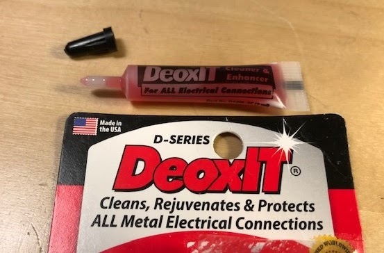
6.  Clean the switch contacts with a contact cleaner.  Use a cotton swab to clean the contacts inside the switch case.  (Note:  I instead sprayed the inside of each switch housing with compressed air (after first removing its plunger) to blow out any debris, and then I put drops of DeoxIT on all of the plunger's contacts before re-inserting the plunger back into its housing.  And if you do use a cotton swab to clean out the inside of the switch housing, I would recommend that it be lint-free so that no fibers remain within the housing after swabbing.)


7.  Return the switch plunger to the main switch case by inserting it and pushing it completely down.

8.  Re-insert the metal or plastic latch, if removed.

9.  Return the PCB to the instrument case (not necessary in my case).

For reference, here's a plunger properly oriented for insertion into its housing (note that the contacts are along the lower sides of the plunger, not the upper sides).


And here's a plunger, upside down.  Note the springs!  Be careful when touching the contacts -- if a contact falls out, the spring will leap away!  (Been there, done that.  And luckily found the spring in the carpet).


(By the way -- now might be a good time to also add a drop or two of DeoxIT to the contacts of the Input Selection switch.)


With the switches cleaned and my repairs finished, it was time to do a "mini" calibration of the 3438A.


Calibration:

Per the Operating and Service Manual (section 5), calibration requires an HP 740B DC Calibrator and an HP 745A AC Calibrator.  I have neither of these.  Fortunately, one can perform a DC calibration without a 740B, as long as you have a second DVM whose accuracy you trust.

AC Calibration, however, can be an issue if you don't have an AC Calibrator (such as an HP 745A), because three of the adjustment procedures require 19 VRMS AC signals at frequencies of 200 Hz, 20 KHz, and 100 KHz., which I cannot currently provide.  Thus, for the moment, I've skipped these three adjustments.

So consider this my abbreviated, "mini," calibration.

The manual's calibration steps are:

1A: +7V Power Supply Adjustment.   (Procedure is self-explanatory in manual).

1B:  U725 Back Gate Bias Adjustment.  (Procedure is self-explanatory in manual.  Note that the JMVB measurement "loop" is just to the right of C611, at the upper left-hand corner of the R603 potentiometer).

2:  Clock Frequency Adjustment.  (Procedure is self-explanatory in manual).

3:  AC Zero Adjustment.  (Procedure is self-explanatory in manual).

4.  20 Ohms Zero Adjustment.  (Procedure is self-explanatory in manual).

5.  DC Gain Adjustment.  To make this measurement I use an external variable DC supply and connect its output to both the HP 3438A that I am calibrating and to my more accurate HP 34401A DVM.  I then adjust the power supply for about 19 VDC and adjust R403 so that the reading on the 3438A is the same as  the reading on my 34401A.

6.  Ohms Gain Adjustment.  I first verify that a resistor's value is close to 19 Kohms on the HP 34401A. I note its measured value and then I remove this resistor from the 34401A and connect it to the 3438A.  Then, following the steps in the manual, I adjust R119 so that the value displayed on the 3438A equals the value measured on the 34401A.

7.  AC Gain Adjustment.  (This step requires a 19 VRMS, 200 Hz AC source, which I do not have.  So I have skipped this step).

8.  20V AC Range, 20 KHz Adjustment.  (This step requires a 19 VRMS, 20 KHz AC source, which I do not have.  So I have skipped this step).

9.  2V AC  Range, 20 KHz Adjustment.  To make this measurement I use an HP 8904A Function Generator and connect its output to both the HP 3438A that I am calibrating and to my more accurate HP 34401A DVM.  I then set the 8904A to give me a 1.9 VRMS sine wave signal at a frequency of 20KHz.  I then adjust R110 so that the reading on the 3438A is the same as the one measured on the 34401A.

10.  20V AC Range, 100 KHz Adjustment.  (This step requires a 19 VRMS, 100 KHz AC source, which I do not have.  So I have skipped this step).
A note regarding the skipped AC adjustments -- if you have an audio power amplifier that can provide a low-distortion 19 VRMS signal into a high-impedance load, over the frequency range of 200 Hz to 100 KHz, and an appropriate sine-wave generator with which to drive the power amplifier, you can perform the three AC adjustments, above, that I skipped.  Simply drive the 3438A in parallel with a more accurate AC voltmeter (e.g. HP 34401A), and adjust the 3438A until its reading matches the 34401A's reading.

Other Notes:  Noise Pickup:

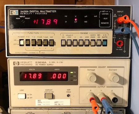
I noticed while I was photographing my 3438A (for the photo at the top of this post in which the 3438A displays +17.89 VDC), that the voltage reading was continually bouncing around between 17.86 to 17.91 volts, rather than being a steady 17.89 volts.

I initially thought there was a noise issue with the circuitry inside the meter, but when I moved the 3438A to my desktop from its original position on top of the HP E3616A DC Power Supply (while keeping it attached to the E3616A generating 17.89 volts), the display settled down.

My conclusion is that the meter is somehow sensitive to stray magnetic-field pickup, such as the B-field from the E3616A's power transformer.  Moving the meter away from the E3616A power-supply fixed the problem.


Resources:

Although Keysight provides a free 3438A Operating and Service PDF on their website, its schematics are unreadable and thus useless.

Fortunately, one can purchase a readable manual from Artek Manuals:  http://artekmanuals.com/
(Note:  When I purchased Artek's 3438A manual as a PDF download, it also included a PDF of the 3438A-5A Service Note).


Standard Caveat:

I might have made a mistake in my designs, schematics, equations, models, etc.  If anything looks confusing or wrong to you, please feel free to leave a comment or send me an email.

Also, I will note:

This design and any associated information is distributed in the hope that it will be useful, but WITHOUT ANY WARRANTY; without an implied warranty of MERCHANTABILITY or FITNESS FOR A PARTICULAR PURPOSE.
Wednesday, January 1, 2020

VNA: Notes on THRU-standard de-embedding


Note:  This blog post is a continuation of the topic of VNA Error Correction, which I first discuss (with a dive into "Twelve-term Error Correction") here.  I recommend first reviewing that post before delving into this one.

Prior to performing VNA measurements on a two-port device, a VNA's calibration steps will often include using a THRU adapter (such as a barrel-connector) to connect together the cables attached to the VNA's two ports to complete the end-to-end calibration process.  Following calibration, the THRU adapter is removed and the DUT (Device-Under-Test) is connected in its place, ready for its S-parameter measurements.

If the THRU adapter is not ideal (e.g. it has length (i.e. delay) and/or loss or mismatch), these impairments will affect four of the twelve error-terms calculated during calibration. 

Because the THRU adapter is removed after calibration (before DUT measurements are made), there needs to be a way to remove the effect its impairments have had on these four error terms derived during calibration when the THRU was present.  After all, with the THRU removed, its deficiencies are no longer present in the test setup, and thus they should not be included in the 12-term error model.  If these effects are not removed, the two-port measurements of the DUT will be incorrect.

HP's VNAs (e.g 8753 series) typically assume that the THRU used during calibration is ideal -- it has zero length and thus no delay.  However, these VNAs also allow the user to modify the THRU's definition to include non-ideal characteristics of the THRU used for calibration.  And their VNA software mathematically removes the effects on calibration that result from these non-ideal characteristics.

I wondered how this "de-embedding" of the THRU from the cal results was done.  A Google search turned up little -- the one document I found had errors, so its math was suspect.  So, I decided to tackle the math myself, using the 12-term error model equations in my previous blog post (here).

And thus this post!  Before getting into the math, though, let's first build a foundation...


Compensating for a non-Ideal THRU standard:

The HP 8753D User's Guide contains the following note regarding THRU connections:


In other words, if a THRU adapter is used, the HP VNA needs to know its characteristics (deficiencies) so that it can remove their effect when the THRU is removed and the DUT inserted in its place.

First, though, let's start with a definition of an "ideal" THRU:

An Ideal "Zero-Length" THRU:

A "zero-length" THRU exists when "sexless" connectors are connected together (such as APC-7 connectors), or, perhaps more commonly, when one cable has a male connector and the other a female connector, as shown, below:


An ideal THRU, having no delay or other deficiencies, does not require the VNA to make any additional adjustments to the VNA's 12-term error model when the DUT is inserted into the test system in place of the "ideal" THRU.


A Non-Ideal THRU:

For systems in which the two measurement ports have the same-sexed connector (.e.g both are male SMA connectors), a THRU adapter must be used.  But this adapter, having an actual non-zero length, introduces a delay (and possibly attenuation and/or mismatch) into the measurement:


Basic non-ideal THRU Model:

HP's model for a non-ideal THRU is shown below ([Keysight, Modifying Calibration Kit]):


This model is exactly the same transmission-line model that was used in defining the transmission-line section of the SOL Reflection Standards in my previous blog post, here.

Keysight defines these three Offset parameters to be:

Offset Delay:

For a Thru standard, this is the one-way propagation time (in seconds) from the measurement plane at one end of the Thru to the measurement plane at its other end.

Offset Loss:

Energy loss due to the Transmission Line's skin effect, specified in Ohms/Second at 1 GHz.  Keysight notes that, for many applications, setting this value to zero will not result in significant errors.

Offset Zo:

Per Keysight,"The offset impedance between the standard to-be-defined and the actual measurement plane.  Normally, this is set to the system's characteristic impedance."  I.e.  the THRU is assumed to be matched to the characteristic-impedance of the test setup.


And here are the formulas for Keysight's "offset" definitions:


A non-ideal THRU can be represented by a 2x2 S-parameter matrix whose elements are functions of these three "offset" terms defined by Keysight.  If the THRU were ideal, these four parameters would be:  S11 = S22 = 0, and S21 = S12 = 1.  A non-ideal THRU will have different S-parameter values.


Two-Port Measurement Error Terms:

Four of the twelve error-terms calculated during the VNA's calibration phase are errors calculated when Port 1 of the VNA is connected to Port 2 of the VNA.  These four errors are:  e22, e'11, e10e32, and e'23e'01.

These four error terms are the errors related to Port-to-port Transmission and Reflection, and they correspond to the following error-terms in the HP 8753D Manual's model:
  • e22 = ELF  (Load Match of Port 2 as seen at Port 1)
  • e10e32 = ETF  (Transmission Tracking, Port 1 to Port 2)
  • e'11 = ELR   (Load Match of Port 1 as seen at Port 2)
  • e'23e'01 = ETR (Transmission Tracking, Port 2 to Port 1)


In my previous blog post (which discusses how to find the twelve error terms, see here), it is assumed that these last four errors are determined when the two ports of the VNA are connected together with an ideal THRU (i.e. the THRU's S11 and S22 equal 0 and its S21 and S12 equal 1).

But suppose the two VNA ports are connected together with a non-ideal THRU that has loss, delay, and/or impedance mismatch.  For example, a barrel connector?  If we use the equations derived in the previous blog post, the results for the four error terms will be incorrect.  

We must derive new equations.

To derive these equations, I am going to assume that the THRU's s-parameters are known.  They have already been determined (e.g. either by measurement and calculation or by the THRU's manufacturer).  

Let's call the THRU's s-parameters:  S11T, S21T, S22T, S12T (where the 'T' stands for "THRU").

Given this known THRU and the other eight error terms (calculated during the calibration procedure before we connect the two VNA ports together with the THRU, see here), how do we find e22, e'11, e10e32, and e'23e'01 during the last phase of calibration, given a non-ideal, but fully characterized, THRU?


Equations for Two-port Errors e22 and e10e32:

To derive the equations for the two error terms relating to Port 1 as driver and Port 2 as receiver (e22 and e10e32), let's take a look at Doug Rytting's "Forward Model" that I presented in my previous post, here.


We can replace the unknown DUT in the drawing above with our known (i.e. characterized) THRU, as shown, below:


Note that S11T, S21T, S22T, and S12T are the THRU's known (defined) s-parameters.

If you've read the previous blog post, recall that the previous calibration steps result in all error terms  for this model being calculated except for e22 and e10e32.

And we also already know the THRU's s-parameters.  Therefore, the equations (in the above drawing) for S11M and S21M only have one unknown each.  The unknown for the S11M equation is e22, and the unknown for the S21M equation is e10e32.

So, using algebra, we can rearrange the S11M equation to give us an equation for e22, and we can rearrange the S21M equation to give use an equation for e10e32. (The latter is easily derived. The former requires a bit more pencil pushing).  These two new equations are:


(If you solve these equations assuming the THRU is ideal (S11T = S22T = 0, S21T = S12T = 1), these equations reduce to equations (9) and (10) in my previous blog post, here.)


Equations for Two-port Errors e'11 and e'23e'01:

Similarly, we can derive the equations for the two error terms relating to Port 2 as driver and Port 1 as receiver (e'11 and e'23e'01).

This time we will use Doug Rytting's "Reverse Model" that I presented in my previous post, here.


Again, let us replace the unknown DUT in the drawing, above, with our characterized THRU:


And we can rearrange the equations for S22M and S12M to give us new equations for e'11 and e'23e'01:


(If you solve these equations assuming the THRU is ideal (S11T = S22T = 0, S21T = S12T = 1), these equations reduce to equations (11) and (12) in my previous blog post, here.)


And that's it!  We now have four equations with which we can calculate the last four of the twelve error terms, given calibration with a non-ideal, but characterized, THRU.


Conclusion:

In my previous blog post (here) I discuss equations for calculating the four VNA error terms relating to VNA transmission errors: e22, e'11, e10e32, and e'23e'01.  But these equations assumed that the THRU connecting the two VNA ports was ideal -- that is, it had neither loss nor delay, and its characteristic-impedance was matched to the system.

But quite often we use non-ideal THRUs to connect the two VNA ports together during VNA calibration.  An example of a non-ideal THRU is a barrel-connector.  

And if the THRU used for calibration is not ideal and the VNA software assumed that the THRU was ideal, then, if we used the equations in the previous post to calculate e22, e'11, e10e32, and e'23e'01, their calculated values would be wrong.

In this blog post I derive four new equations that allow the correct calculation of e22, e'11, e10e32, and e'23e'01 even if the THRU used during calibration is not ideal.  The only requirement is that the THRU's impairments (loss, delay, and or impedance mismatch) are defined and expressed as S11, S12, S21, and S22. 


A Note on Determining THRU Delay:

Arguably the most important THRU parameter to accurately define is its delay.  To quote Joel Dunsmore (Handbook of Microwave Component Measurements, First Edition, section 3.3.3.3), "Failure to account for the delay of the thru (and to a lesser extent, the loss of the thru) is one of the most common causes of error in RF measurements." 

But suppose our THRU has not been characterized.  How do we determine its delay?

One technique requires the use of both male and female SHORT standards whose own delay has been accurately characterized.  The quotes in blue, below, are from the Keysight "community" website (here) from Dr_Joel:

If you have a f-f adapter, you can modify the cal kit to add the delay of the adapter to the calkit and then it will work fine for calibration.  A typical SMA "bullet" is about 90 psec of delay.

You can measure it directly by doing a 1 port cal, then adding a short from the calkit (this will be the F short), then doing a data->mem and data/mem to normalize out the short delay and get a flat line, change the format to phase.  Then add the SMA bullet (f-f adapter) and put the other sex short (male) on the output and see the phase slope.  You can use port extensions to dial in extension until the slope is flat, then this is the 1-way delay of the adapter. 
 
(This assumes the male SHORT has the same delay as the female SHORT.  If they are different, you will need to compensate for this difference,  k6jca.)

do this from maybe 1 Mhz to 3 Ghz for the freq span (even if your DUT is narrower, as it will give some good phase slope for a short adapter).

It turns out we make the m and f shorts so that they have the same phase and delay in the 3.5 mm case.


Thanks:

A huge thanks to Christian Zietz who took the time to correct my initial approach and derived equations for finding these four error terms given a THRU whose S11T and S22T were 0 (i.e. the THRU although not ideal, is matched).  (Refer to this nanaVNA thread:  https://groups.io/g/nanovna-users/topic/solt_error_theory/77330684?p=,,,20,0,0,0::recentpostdate%2Fsticky,,,20,2,0,77330684)

Christian's thread got me thinking, and, while reviewing Doug Rytting's equations, I realized that they contained the answer for finding these four error terms even if the THRU were mismatched to the system.  All I had to do was replace the original DUT with the known THRU and solve for the error terms.


References:

8753D User Guide – Chapter 6:  Note note regarding Thru length.  Also equations and drawings.

Rumiantsev, VNA Calibration IEEE Mag June 2008 page 86:  Models use similar nomenclature to HP. 

Network_Analyzer_Error_Models_and_Calibration_Methods, Rytting: 1.  Uses e00 etc. to name the error terms.  2.  Does not give equations for solving for e00, e11 and e10e01 (but he does for e22 and e10e32).  3.  Mentions the 4 steps for determining the 12 error terms.  No de-embedding of Thru.

Time-domain thru-reflect-line (TRL) calibration errorassessment:  Nice drawings of FWD and REVERSE models (page 7).

Effect of Loss on VNA Calibration Standards, Monsalve:  Good recapitulation of HP’s lossy-standard equations (i.e. equation for gamma, etc – see Keysight’s “Specifying Calibration Standards and Kits”).

Schreuder – DeEmbed Manual:  A source of equations, but note errors, thus suspect.  Also, I don’t think he properly de-embeds the thru standard.  Includes Thru standard de-embedding (some equations might have errors).

HP Journal 1970-02:  Note that the equations (author Hand) use the e00 terminology.  Note:  does not de-embed the thru (assumed to be ideal).

Improved RF Hardware and Calibration Methods, Rytting: Recapitulation of error terms using ‘e’ nomenclature (e.g. e00).  Does not give equations for solving for e00, etc.  But does introduce “bilinear transform’ for expressing the equation for S11m.  No de-embedding of thru.

Modifying Calibration Kit Definition:  Compact summary of the Reflection Model of Standards.  Note equation for Offset Loss.  (Need to compare to equation in other HP app note).

Error Correction in Vector Network Analyzers, DG8SAQ:  Uses Moebius transform in lieu of the bilinear transform mentioned above (Rytting, Improved RF Hardware and Calibration Methods).

Applying Error Correction to Network AnalyzerMeasurements, Agilent (app note 1287-3):  Summary of 2-port error correction but with error term nomenclature Ed, Es, Ert, etc.

Keysight, Specifying Calibration Standards and Kits, 5989-4840EN:  Good model of 1 port standard.  Also note equations for alpha and beta based upon offset_delay, offset_loss, etc.

MiniCircuits -- Calibration Standards and the SOLTMethod, AN49-017:  Models of 1 port standards (but not thru).  Note equations use tanh.  And also Zc and gamma*length equations.

Agilent, Specifying Calibration Standards for the 8510, 5956-4352: Two port model in terms of Esf, Edf, Erf, etc.  Note method of determing Ceff for open (page 10).

Keysight, Modifying Calibration Kit Definition:  (Good) Models, and definition of terms, for Reflection Standards and Transmission Standard (i.e. Thru).  And note that Thru’s normally considered to be “zero length”

Keysight, In-Fixture Measurements Using Vector Network Analyzers, 5968-5329:  (Good) Describes how to characterize Short, Open, and Load standards. (Note:  Characterizing an Open’s fringing capacitance only necessary above about 300 MHz).  Also interesting Cal fixture w/zero-length Thru.

Agilent, De-embedding and Embedding S-parameter Networks Using a Vector Network Analyzer (app note 1364-1).


Standard Caveat:

I might have made a mistake in my designs, schematics, equations, models, etc.  If anything looks confusing or wrong to you, please feel free to leave a comment or send me an email.

Also, I will note:

This design and any associated information is distributed in the hope that it will be useful, but WITHOUT ANY WARRANTY; without an implied warranty of MERCHANTABILITY or FITNESS FOR A PARTICULAR PURPOSE.