Thursday, September 28, 2017

An FPGA SDR HF Transceiver, Part 10 -- A 30 Amp Switching Power Supply

In this tenth blog post in my FPGA SDR transceiver series I will describe a 30 Amp switching power supply used to power the HF RF PA and the FPGA SDR transceiver.

(Part 9 of the series is here: Part 9).


Before I begin, let me again acknowledge Dick Benson, W1QG.  Dick is the father of this FPGA SDR design, and although I've made some modifications to the FPGA logic, the underlying architecture and the vast majority of the Simulink implementation is Dick's.

A note regarding the schematics...

These schematics were drawn using the Lite version of Cadence's Orcad Capture.  This is the free version of the program, and it limits a schematic's number of nets to 75 and the number of parts to 60 (limitations which apply if you want to save the design, which I always do).

Because this radio design has many more nets and parts than the 75/60 limit specified by Cadence, I have broken the overall design into smaller "bite size" schematics, each  independent of the others and each drawn on a single A-size sheet.

But because I've broken up the design into smaller independent pieces, I can not use Capture's Design Rule Checker to check the overall design for design flaws.  Therefore, there is the possibility that errors have crept into the schematics.  So be aware!


Schematic:

(Click on image to enlarge)

Schematic Notes:

1.  F1, the Corcom 0960-0446 Filter, is the orignal AC Power Inlet plus fuse plus filter that was installed in the HP 37203A unit.  Its filtering consists of an 18 nF cap on the Line side of its filter and 465 uH inductors in the Live and in the Neutral AC line wires.  You can see its schematic in the image, below.


2. F2 is a Corcom 10VW1 AC Line filter:


3.  Ferrite Beads FB1 and FB4 are common-mode chokes, and each consists of a single turn through a Fair-Rite 26354-0002 ferrite core.

4.  Ferrite Beads FB2 and FB3 are common-mode chokes on the DC output side of the supply, each consisting of 2 turns around a Fair-Rite 2643102002 ferrite core.  (At least I believe they are 2643102002 cores -- they were in a bag marked "43?" in my junk-box.  You can see them below, in a shot of the inside of the back panel.)


 By the way, '31' ferrite material might be a better choice for this application than '43' ferrite.

5.  The Power Switch, SW1, is the HP chassis' original power switch.

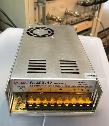
6.  The heart of this supply is a commercially available switching power supply, the MegaWatt S-400-12.  At this time, this supply can be purchased via Amazon.  Note that Amazon sells other supplies with the same specs and whose case look identical to the MegaWatt supply for much lower prices.  Are these switchers equivalent?  I have no idea.  But I would be suspicious that parts might have been removed (not stuffed) in an effort to get the price down.

Here is a picture of my MegaWatt Switcher:


And inside the MegaWatt switcher:


 (If you purchase a less expensive knock-off supply, the the EMI-suppression components might have been removed to reduce cost.  You can compare your supply to the image above, in which the EMI suppression components are located in the bottom half of the picture).


Build Notes:

Again, I have used an old HP 37203A "HP-IB Extender" Chassis to house this switching supply.

A view into the top of the chassis.  (The hand written note tells me to use a larger screw in that corner of the power supply due to stripped threads -- oops!).


The MegaWatt switcher is mounted onto a non-conductive plexiglass plate.  I had earlier noticed, during bench testing, that the FPGA SDR had some in-ham-band EMI spurs when the RF PA was stacked directly on top of the MegaWatt switcher so that the PA's heat-sink fins were in direct electrical contact with the MegaWatt case.

I discovered that if I put a piece of paper between the PA heat-sink and the switcher case so that they no longer had direct electrical and physical contact, the spurs went away.

So clearly there was some sort of unwanted noise path between the PA ground (i.e. heat-sink) and the switcher's case (the supply's AC protective ground) and switcher noise was probably being conducted along the shield of the PA's coaxial cable, and thus appearing as receive spurs.

To ensure that the switcher's protective-ground does not have a direct low-impedance AC connection to the PA ground, I mounted the switcher case on a non-conductive piece of plexiglass and then I fed its protective-ground (its chassis ground) through the same ferrite common-mode chokes (baluns) through which the AC Live and Neutral wires pass (refer to schematic).

And on the DC side, the DC output (both plus and minus sides) pass through another set of ferrite common-mode chokes.  Again, to (hopefully) provide a high-impedance path to common-mode switcher noise.

The switcher's internal fan exhausts through the bottom of the HP chassis, and so I've mounted the power supply upside down on the plexiglass plate, with the swither's fan pointed down.


The weather-stripping foam around the fan provides an air seal between the top of the MegaWatt switcher and the HP bottom cover.

A view of the bottom of the HP chassis and the holes for fan exhaust:


The back panel.  Not much there!  The holes provide an air intake path for the MegaWatt switcher's fan.


 Here is the FPGA SDR, the HF RF PA, and the 30A Switching Power Supply, stacked:


And finally, for reference, here's the stack wiring:


Other Notes:

1.  The MegaWatt switcher's fan is a bit noisy.  Some reviews on eHam mention replacing it with a higher quality (quieter) fan.  (Or I might home-brew a fan speed controller.)

2.  EMI:

As a straight-forward test (relatively), let's take a look at noise on the 14V DC out line.

When I first tried this, I saw:


Not great!

But then I did a bit more poking around (spurred on by Dick, W1QG), and discovered that this noise seemed to be introduced by a ground-loop formed by the switcher and scope Protective Grounds (that is, the two devices are connected via the third wire in the AC mains plug), and when the switcher and the scope are also connected together via the scope probe's ground.

By the way, "ground-loop" might not be the right term for this phenomena.

Anyway, I "broke" the loop by "removing" the scope's AC cord's protective ground wire, using this AC adapter:


(Another way to remove noise such as this is to use two scope probes in differential mode).

With the ground loop broken, there is still a bit of noise, but much less than before.  So, let me first establish a scope "baseline" of noise intrinsic to the measurement setup before looking at noise introduced by the switching power supply.

Here's the noise baseline:


Notes on the noise baseline:
  1. The Switching supply is OFF.
  2. The scope signal is AC coupled, so I am just looking at noise, not DC.
  3. The scope probe ground is attached to the switcher's chassis, as is the scope probe, itself.
  4. The scope's AC power cord has had its "protective ground" pin floated by using a 3-pin to 2-pin adapter. 
So there is some amount of baseline noise.  What is its source?  I don't know.

Next, I will turn ON the switcher, which will power up the RF PA and the FPGA SDR.  The scope probe and its ground are still attached to the switcher's chassis.  Here's a shot of the noise now:


No difference that I can see.

Now, let's move the probe over to the 14V DC line while keeping scope probe ground connected to the chassis:


Still not much difference!

But if I zoom out the time-base from 500ns/div to 10us/div, I see something that I did not see when the switcher was off.  A (roughly) 50-60 KHz waveform:


But apart from that, not much additional noise.

Let's see how the noise changes if the switcher is sourcing a lot of power -- in other words, when I am transmitting.

If transmitting (3.865 MHz, CW, 100 watts out), the 50-60 KHz component increases significantly, as shown below.  Note that the vertical scale has been increased by a factor of 10, from 20mv/div to 200mv/div:


EMI comments...

Is the switcher noise audible?  The best way to find out will be to do listening tests with the FPGA SDR receiver, searching for receive spurs/noise that might be generated by the switcher when the switcher is powering both the FPGA SDR transceiver and my Automatic Antenna Tuner.  And the simplest way to do this is to build a power-supply "diode-or" circuit, as shown below, and then, tune across the spectrum in 1 KHz steps with both the Linear and the Switching supply ON.  If I encounter spurs or noise, I would then switch OFF the 30 Amp Switcher supply and check if the spur/noise disappears.  If it is still there, it was not created by the switcher, but if it goes away...switcher artifact!

(Click on image to enlarge)

Circuit built and listening tests performed...

The switcher was set to 14.3 VDC out and the linear supply set to 13.6 VDC out.  A 50 ohm dummy load (ME-165/G ) was switched into the antenna feed-line, and I tuned in 1 KHz steps (in CW mode) listening for strange noises.  (Note that the antenna feed-line is grounded where it exits the shack -- I wanted to maintain this ground connection during this test to see if there was an unwanted ground loop upon which noise would travel along the coax feed-line's shield and by this path introduce noise into the receiver).

The results:

1.  I did not hear any spurs generated by the switcher power supply.

2.  I did hear some very weak spurs, below 2 MHz, that seemed to be related to the FPGA SDR's 5V switching regulators (of which there are two -- one to power the FPGA board and associated circuitry, and the other to power the Arduino and front-panel circuitry).  These spurs were 55 KHz apart, and I am hypothesizing that these spurs are related to one (or both) of the FPGA SDR's 5V switchers because, when I turned off the 14V switching power supply, their frequency shifted slighly, which I am assuming is caused by their input voltage changing from 14.3 VDC to 13.6 VDC).


OK.  That's it for this blog post!


Background Notes:

SDR Notes:  Weaver Modulation and Demodulation
SDR Notes:  The Mixer Mathematics of Digital Down Conversion


Posts in this Series:

Part 1: Overview
Part 2: FPGA Modulation and Demodulation
Part 3: Interpolation and Decimation Filters
Part 5: Control Interface, Etc.
Part 9: 50 dB HF RF Power Amplifier


Standard Caveat:

I might have made a mistake in my designs, equations, schematics, models, etc.  If anything looks confusing or wrong to you, please feel free to comment below or send me an email.

Also, I will note:

This design and any associated information is distributed in the hope that it will be useful, but WITHOUT ANY WARRANTY; without even the implied warranty of MERCHANTABILITY or FITNESS FOR A PARTICULAR PURPOSE.

Wednesday, September 27, 2017

An FPGA SDR HF Transceiver, Part 9 -- A 50 dB HF RF Power Amplifier

In this ninth blog post in my FPGA SDR transceiver series I will describe the RF Power Amplifier used to amplify the FPGA SDR's 0 dBm (1 milliwatt) output signal up to 50 dBm out (100 watts).

(Part 8 of the series is here: Part 8).


The HF RF PA is shown above, below the K6JCA FPGA SDR transceiver.

Before I begin, let me again acknowledge Dick Benson, W1QG.  Dick is the father of this FPGA SDR design, and although I've made some modifications to the FPGA logic, the underlying architecture and the vast majority of the Simulink implementation is Dick's.

A note regarding the schematics...

These schematics were drawn using the Lite version of Cadence's Orcad Capture.  This is the free version of the program, and it limits a schematic's number of nets to 75 and the number of parts to 60 (limitations which apply if you want to save the design, which I always do).

Because this radio design has many more nets and parts than the 75/60 limit specified by Cadence, I have broken the overall design into smaller "bite size" schematics, each  independent of the others and each drawn on a single A-size sheet.

But because I've broken up the design into smaller independent pieces, I can not use Capture's Design Rule Checker to check the overall design for design flaws.  Therefore, there is the possibility that errors have crept into the schematics.  So be aware!

Note:  This Post in a Work in Progress and thus
Not Yet Finished!

Summary:

The HF RF PA amplifies the FPGA SDR's 0 dBm output signal up to 50 dBm (100 watts) in two stages.  The first stage is a PA driver amplifying the TX signal by about 30 dB (from 0 dBm to 30 dBm), and the second stage is a Power Amplifier that amplifies the 30 dBm signal from the driver  by about 20 dB (depending upon band) to achieve the final output power of 50 dBm (100 watts).  This second stage consists of a Flexradio SDR-1000 PA Module from an SDR-1000 transceiver.

PA voltage is 14 VDC (or, if one prefers, 13.8 VDC).

You might be wondering -- why did I install the 30 dB driver stage in this amplifier chassis and not in the FPGA SDR transceiver chassis?

The main reason is: control of the 30 dB driver's load impedance.  The SDR-1000 PA's input impedance is not 50 ohms (at least, not on the higher bands).  Thus, if there is a length of 50 ohm coax between the driver's output and the SDR-1000 PA input, the 30 dB Driver's load impedance will change as a function of coax length.

So, I thought it better to have this length of coax be fixed, rather than be some unknown length, so that system performance would not vary depending upon whatever random length of coax I might happen to use to connect the FPGA SDR transceiver to the PA, if the 30 dB driver were in the transceiver rather than PA chassis.


Block Diagram:

(Click on image to enlarge)

Notes on Block Diagram:
  • 50 dB of amplification is achieved with a 30 dB Driver followed by a 20 dB PA.
  • The 20 dB PA is an SDR-1000 PA Module (Flexradio transceiver).
  • The FPGA SDR transceiver controls the driver and SDR-1000 PA module via an 8-wire (plus shield) parallel interface, implemented with an RJ-45 connector.  This interface selects the appropriate band-specific low-pass output filter and also carries the T/R signal.
  • The 30 dB driver is switched in-line during transmit.  During receive this driver is bypassed, and the RF In and RF Out connectors are connected together without any amplification or filtering in-line -- the receive signal pass directly from the "RF Out" connector to the "RF In" connector (and to the FPGA SDR) without modification.
  • 14VDC from the rear panel goes directly to the SDR-1000 PA, where it is fused (25A fuse).  Following this fuse the 14V can power external devices (such as the FPGA SDR) as well as internal circuitry within the PA chassis.

Schematics:

Back Panel Schematic:

(Click on image to enlarge)

Notes on Back Panel Schematic:
  • Several connectors are not used (at this time), but have been installed in anticipation of their incorporation.
  • At the moment, the fan voltage is set to about 7 volts (via the resistors) to ensure that it isn't too loud.  In the future I would like to add a temperature sensor (to the PA heatsink) and use that sensor's output to control the fan's speed.

RJ-45 Control Interface Schematic:

The FPGA SDR controls the HF RF PA via a parallel interface, implemented with an 8-pin shielded RJ-45 connector:

(Click on image to enlarge)

Notes on RJ-45 Control Interface Schematic:
  • The RJ-45 cable must be shielded, as this shield carries the ground-return for the control signals.
  • All 8 wires are connected, although only 7 are used to carry signaling at this time.  (The unused eighth wire is there in case I need to add additional functionality in the future -- for example, if, for some reason, I need to differentiate between between bands that, in the SDR-1000 PA implementation, are paired to share a common low-pass filter at the PA output (e.g. the band-pairs  60/40, 30/20, 17/15, and 12/10 meters).
  • All control signals have simple 1-pole RC low-pass filters to help block external RF from the internal circuitry.  ESD control is also handled with 5V TVS devices (note that the R in the RC filters will current-limit ESD hits on any line).  ESD protection isn't really required in a "one-off" design, but adding such protection was required in a number of commercial products that I designed.  I believe it is a good design habit to have, and I've carried this practice forward into my personal designs.

PA Interface Schematic:

The PA Interface provides the necessary circuitry to allow the RJ-45 interface signals (from the FPGA SDR) to control the PA and PA Driver.  It also provides an interface for internal control to allow this amplifier to be used in stand-alone applications -- control would be handled via front-panel switches (i.e. selecting low-pass filters) and an external T/R input on the back panel -- but note that, at this time, "internal control" of the amplifier has not been implemented.

(Click on image to enlarge)

Notes on PA Interface Schematic:
  • The "External Control" connector attaches to the RJ-45 Interface (see earlier schematic) via a 16-pin cable, and it is the port through which the FPGA SDR controls the PA.
  • The "Internal Control" connector can connect "local" (front-panel) controls to the PA and thus could allow the amplifier to be used in stand-alone applications without the FPGA SDR transceiver being attached to its "External Control" interface.  (At the moment, though, there are no "local" controls).
  • Given that there are no "local" controls at this moment, J16 should be shorted -- this signal, when low, tells the FPGA SDR transceiver that it is connected to the PA.  (If there were local controls, this signal would be forced high if the PA were placed in "local" mode, rather than in "FPGA SDR" Control mode).
  • The nPA_EN signal at J8 is not used -- I had intended to have the FPGA SDR drive this signal, to turn ON the bias regulator on the SDR-1000 PA Module (via J5 pin 9), but there was too much current, and thus too much voltage drop, through the various 100 ohm resistors in my EMI-mitigation low-pass filters that I decided to remove this function.  Instead, J5 pin 9 now connects to the drain of Q8, a 2N7000 that, during Transmit, pulls J5 pin 9 low and turns ON the PA bias.  Header J18 is there in case I want to force the PA Bias to be ON (by shorting the two header pins).
  • At J5, the PAF0 - PAF2 bits select the SDR-1000 PA module's output lowpass filter (per the table shown on the schematic page), while PATR is the T/R signal (high = transmit).  These signals are driven by a ULN2003 IC in the SDR FPGA radio -- an open collector driver which inverts them from their "high-true" sense, and these signals are inverted here again (back to their original sense) using 2N3905 PNP transistors.  Bypass caps across the transistors' base-emitter junctions, as well as from the collectors to ground, to shunt RF off of these lines (or junctions) and thus help mitigate any issues caused by RF pickup.
  • At J8, nEXT_CTRL is meant to allow the FPGA SDR transceiver to force the PA into "FPGA SDR" control mode, if it had been set to "local" control mode via the PA's (currently non-existent) front panel controls.
  • At J7, nDRVR_BYPASS is meant to allow the 30 dB Driver stage to be bypassed (when in "local" control mode), in case this PA were to be used in a stand-alone application for which that extra 30 dB of drive was not needed -- for example, to amplify a 1 watt QRP transceiver's output.
  • At the moment the 5V connector, J17, is not used.  It is there to power any "Internal Control" circuitry that I might want to add to this design in the future.
  • I'm not using the FlexRadio PA's directional coupler (with its on-board ADC), so the three control pins for this ADC (located at J5, pins 4, 5, and 6) are all pulled HIGH.

PA Driver Interface Schematic:

The PA Driver Interface switches the PA Driver into and out of the signal path.  During transmit it is in the signal path, and during receive it is bypassed.

(Click on image to enlarge)

Notes on PA Driver Interface Schematic:
  • The PA Driver (discussed below) is powered by 12 VDC (the OPA2674's "Absolute Maximum" power supply rating is 13.0 VDC) , and I use an LM2940 low-dropout regulator (LDO) to create 12 volts from the 14 volts used to power the PA.  But note that this LDO is actually mounted on the PA Driver board heatsink, not on the PA Driver Interface board.
  • LDO regulators can suffer from loop instability and usually require that the ESR of their output capacitor(s) be within a certain range (refer to section 8.2.2.1.2 in the LM2940 datasheet).  I'm using a Kemet T491D476M016AT 47uF, 16V, Tantalum cap, whose ESR is spec'd at 800 milliohms.
  • 1N4148 diodes clamp the back-voltage across each relay coil when that coil is "released".  

PA Driver Schematic:

The PA Driver provides 30 dB (or so) of low-distortion amplification of the FPGA SDR's 0 dBm output signal.

(Click on image to enlarge)

Notes on PA Driver Schematic:

Front Panel Schematic:

The front panel is simplicity itself and consists only of two LEDs.  A green LED illuminates when the PA is powered up, and a red LED illuminates during Transmit.

(Click on image to enlarge)

(No notes on the Front Panel Schematic.)


FlexRadio SDR-1000 PA Mods:

While testing the PA Module in my chassis I discovered that the FlexRadio PA's LPF-select relays would chatter (or erroneously turn ON) on some bands, at some power levels.

To help quench this RFI issue, I stiffened up the filtering on the three PAF bits (used to select the LPF to be used for a specific band) by paralleling the existing 10 NF caps with 100 NF caps.  (These signals can be heavily loaded with capacitance because their timing is not critical -- they only change when the user selects a new band).

The modification is shown, below.

(Click on image to enlarge)


Implementation:

I built the PA into an old HP 37203A HP-IB Extender chassis (this is the same type of chassis that I used for the FPGA SDR transceiver).

Top View:


Notes on Overall Implementation:
  • The PA Interface board and the SDR-1000 PA Module are mounted on a piece of PCB copper-clad board that serves as a bottom mounting plate.
  • The PA Driver and PA Driver Interface are mounted to the side of the chassis.

Driver and Driver Interface:


Notes on Driver and Driver Interface Implementation:
  • The LM2940 LDO is at the left of the picture above, soldered to a copper sheet used as a heatsink.
  • The copper sheet also bends up and is soldered to the PA Driver board -- several pennies are soldered to the copper plane on the backside of the Driver board (under the OPA2674 drivers) to conduct heat from the back of the board.  The copper sheet is soldered to the other side of these pennies.  Thus, heat is conducted from the back side of the driver board, through the pennies, and to the copper sheet which is screwed to the HP chassis side rails.  (Note that pre-1982 pennies have a much higher copper content than later pennies, and thus I prefer them for their heat transfer characteristics).

Back Panel:


(No notes on the back panel.)


PA Interface:


Notes on PA Interface Implementation:
  • There are some surface mount LEDs visible -- these are not used.
  • This picture was taken before I added the three PNP inverters for the three PAF signals.

Notes on Performance:

1.  DAC rolloff:

The frequency response of Digital to Analog Converters (DACs) is not flat, but rolls off according to the following sin(x)/x formula:

H(f) = sin(πf/fs)/(πf/fs)

Given the FPGA SDR's sampling rate (fs) of 80 Mega-samples/second, then the DAC output will be down 0.5 dB at 14.35 MHz, 1.0 dB at 21.2 MHz, 1.4 dB at 24.7 MHz, and 2.1 dB at 29.7 MHz.

 (For more on DAC sin(x)/x rolloff, go here: https://www.maximintegrated.com/en/app-notes/index.mvp/id/3853 or here:
http://www.atx7006.com/articles/dac_frequency_response


2.  PA IMD Measurements:

(Click on image to enlarge)

(Click on image to enlarge)

Notes on PA IMD Measurements:
  1. I'm only going to measure 3rd order IMD, not higher orders.
  2. The value "% of Max SDR Drive" is the amount of "possible" drive (in terms of voltage level) from the SDR's transmitter that, with this SDR-1000 PA, results in 100 watts out (roughly).  Note that the maximum output from the SDR FPGA is 0 dBm (and this drops slightly as frequency increases due to sinx/x rolloff).
  3. "Power Out" is measured with an LP-100 Digital Vector RF Wattmeter.
  4. The "Two-Tone Fundamental" is the measured amplitude of one of the two two-tones on the HP 8568B Spectrum Analyzer.
  5. The "Delta to 3rd Order Spur" is the delta in amplitude from either of the two-tone amplitudes (the value in the previous column) to the 3rd order spur.
  6. TX IMD, referenced to two-tone PEP power (the latter being 6 dB above either of the two-tone amplitudes).
  7. Measuring "120 VAC Input Power" from the AC line gives me a rough idea of PA efficiency.  (Note that this value also includes power to the FPGA SDR as well as the LP-100 Wattmeter).
  8. IMD generally worsens as frequency increases except for 160 Meters, which has significantly worse IMD compared to 80 - 15 meters (note that the 120 VAC watts is quite high, too).  This might indicate a problem with the 160 meter Low-Pass Filter, for example.
  9. 100 watts of two-tone PEP power, fed through a 50 dB attenuator, should result in the level of each of the two-tone signals, at the 8568B Spectrum Analyzer, at -6.0 dB.  But they aren't -- this error might be due to 8568B calibration error, LP-100 calibration error, the 50 dB attenuator not being exactly 50 dB, or something else.  But the measurements are close enough to -6 dBm for my purposes.
You will note that I measured 10 meter IMD at an output power of 80 (rather than 100) watts to keep the IMD from worsening much more compared to the other HF bands.  The table below shows how 10 meter TX IMD worsens with output power:

(Click on image to enlarge)

For the same reason, I limited the maximum power on 12 meters to about 90 watts.


3.  Driver IMD Measurements:

Which functional TX block contributes the most to TX IMD -- the driver or the PA?  Let's verify.

Here's the test setup:

(Click on image to enlarge)

(The "Homebrew Directional Coupler" is described here: http://k6jca.blogspot.com/2015/01/building-hf-directional-coupler.html).

And here are the measurements.  The Driver's IMD is shown in the very last column.

(Click on image to enlarge)

Clearly, IMD performance is limited by the PA, not the driver, even on 10 meters.


Future Additions:

Some future additions that I plan to incorporate in...the future:
  1. Fan controller and temperature monitor
  2. External Speaker on the Front Panel.
  3. Local controls for stand-alone PA applications

OK.  That's it for this blog post!

Background Notes:

SDR Notes:  Weaver Modulation and Demodulation
SDR Notes:  The Mixer Mathematics of Digital Down Conversion


Posts in this Series:

Part 1: Overview
Part 2: FPGA Modulation and Demodulation
Part 3: Interpolation and Decimation Filters
Part 5: Control Interface, Etc.
Part 9: 50 dB HF RF Power Amplifier


Standard Caveat:

I might have made a mistake in my designs, equations, schematics, models, etc.  If anything looks confusing or wrong to you, please feel free to comment below or send me an email.

Also, I will note:

This design and any associated information is distributed in the hope that it will be useful, but WITHOUT ANY WARRANTY; without even the implied warranty of MERCHANTABILITY or FITNESS FOR A PARTICULAR PURPOSE.

Wednesday, August 16, 2017

An FPGA SDR HF Transceiver, Part 8 -- Front Panel, Rear Panel, and Other Schematics

In this eighth blog post in my FPGA SDR Transceiver series, I will describe the Front Panel and its Arduino processor (and associated circuitry), the Rear Panel, and other circuitry within the radio that interconnects front panel with rear panel.

(Part 7 of this series is here: Part 7)


Before I begin, let me again acknowledge Dick Benson, W1QG.  Dick is the father of this design, and although I've made some modifications to the FPGA logic, the underlying architecture and the vast majority of the Simulink implementation is Dick's.


A note regarding the schematics...

These schematics were drawn using the Lite version of Cadence's Orcad Capture.  This is the free version of the program, and it limits a schematic's number of nets to 75 and the number of parts to 60 (limitations which apply if you want to save the design, which I always do).

Because this radio design has many more nets and parts than the 75/60 limit specified by Cadence, I have broken the overall design into smaller "bite size" schematics, each  independent of the others and each drawn on a single A-size sheet.

But because I've broken up the design into smaller independent pieces, I can not use Capture's Design Rule Checker to check the overall design for design flaws.  Therefore, there is the possibility that errors have crept into the schematics.  So be aware!


Summary:

The Front Panel provides the User Interface for the radio, and it is designed to be a separate sub-assembly that can easily be removed from the chassis.

An Arduino Nano processor provides the user-interface processing, and it is tasked with reading the front and rear panel controls, displaying information on the LCD, and communicating with the FPGA.

Let's take a look at the schematics...


Front Panel Main (Nano) Board Schematics:

(Click on image to enlarge)

Notes on the "Main" board schematic:
  1. +12V is supplied to the board via J11 in the lower right-hand corner.  This +12V will also power the FPGA board (via header J1).
  2. +5V is also supplied to the board from a separate source (via J12) -- the Arduino Nano's on-board 5V regulator cannot supply the current required at 5V for the front panel, and so a separate switching power supply provides this assembly's 5V power.
  3. J1 is the primary interface to the FPGA board, and it supports the 4-wire Control Interface, provides +12V to the FPGA board, and carries other miscellaneous IO signals (such as mic audio) between the FPGA board and the Front Panel.
  4. Note that the FPGA Control Interface is a 3.3V interface, whereas the Arduino's IOs are 5V.  R9 and R10 (in conjunction with terminating resistors on the FPGA board) divide down the 5V control signals sent from the Arduino to be 3.3V compliant for the FPGA, and U2 and U3 provide a level translation of FPGA 3.3V output signals to input levels compatible with the Arduino's 5V IO. (Note that the Arduino's ViH spec is 3.0V, minimum, which is slightly higher than the Xilinx FPGA minimum VoH spec of 2.9V.  Thus the level translators to ensure that the Xilinx outputs meet the Arduino's ViH spec.) 
  5. U4 provides 3.3 volts for the Main board.
  6. The front panel's Volume control provides a voltage that is converted to digital by the Arduino (and then sent to the FPGA via the 4-wire Command Interface).
  7. Transmit SWR and Forward Power can also be sampled by the Arduino's ADC via connector J6.  (At this time this feature is not used for monitoring power and SWR.  Instead, these pins are used to measure the input DC Voltage (e.g. 13.5 VDC).  This feature is described further, below, in the Interconnects 1 notes).
  8. The board also has a buzzer, LS1, to provide various beeps when I press buttons or when error conditions occur.  The Arduino pin driving this beeper can also be used to "calibrate" the Arduino's ADC readings  (to compensate for the actual ADC reference voltage -- necessary if trying to use VRL and VF to calculate SWR and Forward Power).  Its function is selected via header J10.
  9. There are simple one-pole RC filters on many of the IO signals to mitigate susceptibility to RF fields that might be coupled onto external cabling and leads.
  10. LED D2 is an on-board LED used only for debugging and is not visible during normal radio operation (its function is duplicated by a second LED, to be described later, below).

(Click on image to enlarge)

Notes on the "IO1" Schematic:
  1. This schematic shows two headers that provide IO signals to the Arduino.
  2. The upper header, J21, connects to the rotary encoder used for frequency tuning (this is an Oak/Grigby Rotary Optical Encoder, Model 91Q128-43-00110, that provides 128 pulses per revolution).
  3. The lower header, J22, connects to the two front-panel mechanical rotary encoders and the analog meter.  These rotary encoders include push-button switches and are used to select menu items via the LCD.  (They are similar to those used in the Keyes KY-040 rotary encoder module).
  4. Again, simple one-pole RC filters attenuate any RF that might be coupled into the circuitry via external wiring.

(Click on image to enlarge)

Notes on the "IO2" Schematic:
  1. There are more IO signals than there are Arduino IO pins: U1 is an IO expander (PCF8575) that allows the Nano access to the additional IO signals.  It communicates with the Arduino Nano via the Nano's I2C interface.
  2. The RST signal from U1 is a high-true Reset signal, sent to the FPGA board, used for resetting the FPGA's Communications Interface.  Note that the PCF8575 cannot drive its output pins high, so a pullup is needed (R23).
  3. The Arduino also communicates with the LCD via I2C (using an external I2C to parallel converter mounted at the LCD).  Header J2 provides this interface.
  4. Header J16 provides an extra I2C connector.  It is not used at this time.
  5. The microphone audio attaches to the Arduino board via header J13.  Note that the microphone audio is not used by the Arduino -- instead, this signal is simply routed to the 26-pin FPGA interface connector, where it is sent to the FPGA board (and converted into a digital signal).  By the way, this MIC_AUD signal is not from the mic connector itself, but from a separate mic preamp board that will be described later, below).
  6. U4 provides "clean" 5V that can be used to power an active (FET) mic element.  This feature is not used at this time.
  7. Transmitter keying is controlled via the Arduino, and the signal nPTT (low true) is used both in CW and Voice modes to signal the FPGA (via the Arduino) to Transmit.  Because this signal can come from the outside world, I've added ESD protection with TVS1.  (R8 provides both RF filtering and current-limiting if TVS1 were to clamp).
  8. And again, numerous simple RC filters on control lines to filter out RF that might be coupled onto cabling.
  9. The LED is only used for debugging and is not visible during normal operation of the radio.

Connector Locations:

For my own records, below are the location of the Main Board's connectors (shown in the three schematics, above):


Front Panel 5V Switcher:

The Front Panel's 5V requirements are supplied by a 5V switcher that converts 12V to 5 VDC.  (I had originally used an LM7805 linear regulator, but, given the 5V rail's load current, the 7805 was getting too hot for comfort even with a large heat-sink, and so I went the switcher route.

This circuit is mounted on a separate board within the Front Panel assembly (it is not on the Arduino "Main" board).

(Click on image to enlarge)

The circuit should be self explanatory.  For additional information refer to the LM2576 datasheet.


Front Panel Controls:

Now let's look at the wiring of most of the front panel's controls.  (The remaining controls will be described in the next section, below).

This circuitry should be self-explanatory...

(Click on image to enlarge)

(Click on image to enlarge) 


Front Panel Controls, Rear Panel, and Interconnects:

Below are the remaining front panel controls and connectors, as well as rear panel connectors and how they all interconnect.

(Click on image to enlarge)

Notes on the "Interconnections 1" schematic:
  1. On the rear panel, diode D1 provides protection against accidental reversing of the power supply voltage.
  2. J15, the "EXT. ON" connector, provides a signal for external devices that is low-true when the FPGA SDR radio is ON. 
  3. J3 provides a PTT port parallel with the front-panel's "Key" and "MIC" (PTT pin) ports.  Note that this signal, nPTT, is low true (low = xmit).
  4. The input DC voltage can be monitored (and thus displayed on the LCD) by the Arduino.  This DC voltage is sampled after the Schottky diode on the rear panel and then divided-by-four.  The resulting voltage, on Header J37, is connected to J6 on the Arduino board via a 3-wire cable.  Either J6 pin 1 or J6 pin 3 can be read by the Arduino's ADC, the ADC reading then multiplied by 4 (and with an offset representing the Schottky Diode D1's Vf drop added to this result) to represent the voltage at J34.

This next schematic, "Interconnects 2", details the audio output interconnections:

(Click on image to enlarge)

Notes on the "Interconnects 2" schematic:
  1. Speaker Audio from the FPGA board comes into this schematic via connector J12 (at bottom of schematic).
  2. LS1 is the radio's internal speaker (mounted on the top cover).
  3. An external speaker can be connected to the radio via J1 on the back panel.  Plugging in an external speaker will turn OFF the radio's internal speaker.  (Important note: the external speaker should be connected only to Tip and Ring of the stereo plug, NOT to ground).
  4. Although a stereo connector (J2) is used for the headphones, they are connected in MONO mode (left and right in parallel).
  5. And because the speaker audio from the FPGA board is differential with DC bias, this differential signal is converted to single-ended for the headphones by using just one side of the differential signal (against ground).  The DC bias is removed by C1 (i.e. the audio is AC-coupled to the headphone jack).
  6. R3 keeps the negative side of C1 at ground potential so that there isn't a loud "pop" in the headphones when they are plugged into J2.
  7. The SPKR ON switch turns ON or OFF any speaker (internal or extenal), but not headphone audio.  One side of this switch is read by the Arduino, and the switch status is sent to the FPGA where it is used to change the audio level when headphones are used.

Below is an image showing the interconnects in the two schematics above.

(Click on image to enlarge)

(Note some singeing on the wires going to J12.  Oops!  Also, J37 was originally a 4 pin header.  It has been trimmed down to 3 pins.)


The next schematic details the small "plate" (actually double-sided PCB stock) upon which two RJ45 connectors are mounted:

(Click on image to enlarge)

Notes on the "RJ-45 Plate" schematic:
  1. The two headers on the left-hand side connect to the main FPGA board (described in post 6 of this blog series).  The "Interconnects 3" and the "Interconnects 4" schematics can be found there.
  2. I plan to use an SDR1000 PA (plus a driver board) to amplify the FPGA SDR Radio's TX output up to 100 watts, peak power.  This PA and driver will be mounted in an external chassis and controlled by the FPGA SDR via connector J1 in the schematic (above), which will connect to the separate PA assembly via a shielded RJ-45 cable.
  3. I also have plans to build an external 500 watt solid-state PA.  Similarly, it will connect to J5 in the schematic (above) via a shielded RJ-45 cable.
  4. To prevent EMI coupled onto external wiring from getting into the radio, all IO from the RJ45 pass through simple one-pole RC filters.  These should be placed as close to the RJ45 connectors as possible.


*** Schematics of additional rear-panel connectors will go here.


I'm using a scrap HP 37203A HP-IB Extender as the chassis for this radio.  The original back panel looked like this:


Currently, it now looks like this:


(Note that I am adding connectors as I need them, so not all connector locations are populated yet).


LCD Adapter:

To minimize Arduino IO pin usage, the Arduino communicates with the Front Panel LCD via its 2-wire I2C interface.

But because the LCD itself does not support I2C, I use an I2C Interface LCD Adapter similar to the one shown below and available via eBay:


This adapter is designed for use with LCD modules having a 16-pin SIP interface connector.  Unfortunately, the LCD module I chose has a 16-pin DIP interface connector.  So I wired an adapter board (that sits on the back of the LCD module) to convert the I2C Adapter's 16-pin SIP wiring to 16-pin DIP wiring:

(Click on image to enlarge)

Microphone Preamp:

Microphones typically generate low-level audio.  Although the FPGA could internally amplify a low level signal coming into it via the 16-bit audio ADC (the AK4554 Codec), this amplification (following the ADC) also increases the noise-floor underlying the microphone audio.

So I've added an external Mic Preamp (prior to the audio codec) with three levels of gain:  26 dB, 16 dB, and 6 dB.  Its circuit is below:

(Click on image to enlarge)

Notes on the Microphone Preamp:
  1. An on-board 5V regulator (U2) provides "clean" power for the preamp circuitry. 
  2. The op-amp (U1) has rail-to-rail outputs.
  3. One half of the op-amp (U1A) is not used.  I prefer not to have floating inputs on ICs, so I've connected it in a non-inverting configuration with its output set to 2.5V.
  4. The MIC IN connector (J2) connect to the front panel microphone jack.
  5. The MIC OUT connector (J1) connects to the Arduino board, which passes the amplified microphone audio to the FPGA board and the audio codec there.
  6. TVS1 provides ESD protection against an ESD event occurring on the external MIC signal.
  7. The circuit originally started out with gains of 0, 10, and 20 dB.  I increased these by 6 dB by paralleling the original R8 (20K ohms) with another 20K (because it's easier to piggyback surface mount components than to remove and replace them), and then changing the input series capacitance from 200 nF (two 100 nF caps in parallel) to 400 nF (four 100 nF caps in parallel), to keep the high-pass cutoff at 40 Hz.

Assembly:

The HP case I'm using for the radio is not large, and so to install the Front Panel and its circuitry some creative assembly was required.  The photos below show what is involved...

First, here is the Front Panel with controls, LCD, encoders, and LCD Adapter and 5V switcher mounted (the 5V switcher is mounted (on standoffs) above the Frequency rotary encoder and the LCD Adapter is mounted (on standoffs) above the LCD module):


Next, mounting (on more standoffs) the Main (Arduino) board and the Mic Preamp board above the LCD Module Adapter and 5V switcher boards:


And finally, connecting all of the cables!

(Oh what a tangled web we weave!)


OK.  That's it for this blog post!


Background Notes:

SDR Notes:  Weaver Modulation and Demodulation
SDR Notes:  The Mixer Mathematics of Digital Down Conversion


Posts in this Series:

Part 1: Overview
Part 2: FPGA Modulation and Demodulation
Part 3: Interpolation and Decimation Filters
Part 5: Control Interface, Etc.
Part 9: 50 dB HF RF Power Amplifier


Standard Caveat:

I or Dick might have made a mistake in our designs, equations, schematics, models, etc.  If anything looks confusing or wrong to you, please feel free to comment below or send me an email.

Also, I will note:

This design and any associated information is distributed in the hope that it will be useful, but WITHOUT ANY WARRANTY; without even the implied warranty of MERCHANTABILITY or FITNESS FOR A PARTICULAR PURPOSE.