Monday, March 21, 2022

Representing a Transmission Line as a 2-Port Network

In this blog post I will derive equations representing a transmission line of characteristic impedance Zo and of length 'l' as a two-port network.  As a result, there will be a total of four different pairs of equations, each pair representing the two-port network in a different way.

These pairs of equation will be:

1.  V and I at Port 2, in terms of V and I at Port 1, for a lossy transmission line.

2.  V and I at Port 1, in terms of V and I at Port 2, for a lossy transmission line.

3.  V and I at Port 2, in terms of V and I at Port 1, for a lossless transmission line.

4. V and I at Port 1, in terms of V and I at Port 2, for a lossless transmission line.

(These last two sets of equations are special cases of the first two sets).

The image below shows these voltages and currents for both the transmission line and its two-port model.


The first two sets of equations that will be derived are summarized by the two matrix equations, below:


To derive the two equations in the first set of these equations, let's start with some fundamental definitions...

 
Some fundamentals:

Assume that the transmission line has on it both a forward voltage wave (traveling from left to right) and an independent reverse voltage wave (traveling from right to left).  At any point on the transmission line these forward and reverse voltage waves create forward and reverse current waves:


If we were to measure the voltage at any point on the line, the voltage we would measure at that point will be the sum of the forward voltage and the reverse voltage at that point.  

Note that the forward voltage and the reverse voltage each has its own amplitude and phase at that point.

Similarly, the current at that point will be the difference between the forward current and the reverse current (because the currents are flowing in opposite directions). 


Recognize that for either the forward wave or the reflected wave, their voltage and currents follow ohms law, independently of the other wave (because of the Principle of Superposition).  E.g. I+ = V+/Zo and I-=V-/Zo, where Zo is the transmission line's characteristic impedance.

So we can write equations for the Total Voltage and Current at each end of the transmission line in terms of the forward and reverse voltages at those points:

We can also express the forward and reverse voltages at either end of the transmission line as functions of the Total Voltage and Current at either end:

I will use equations 1, 2, 3, and 4 (in the figure, above) to derive the two-port network equations, but before I go any further in this derivation, let me first define a transmission line's "Propagation Constant."


Sidebar on the exponential terms e-γl and eγl :

Assuming a sinusoidal signal on the transmission line, the exponential term e-γl  (or eγl) represents the effect on a sine wave's amplitude and phase, due to the transmission line's Propagation Constant, γ, as that wave travels along the transmission line.

The other variable in the exponent is 'l', which represents the length that the wave has traveled (or will travel) along the transmission line.

The Propagation Constant is a complex number: γ = α + jβ, where α represents a "real" change in signal amplitude (either positive or negative, i.e. attenuation or gain), and jβ represents a phase shift of the sinusoidal signal, either a positive phase shift or a negative phase shift.  

Both of these values are in terms of unit-length, and so when substituted into the exponential, multiplying α by the length of the line gives overall attenuation (or gain, depending upon reference point), and multiplying jβ by length gives phase-shift for the wave's journey along a defined length of line.

If we were to take a snapshot in time and simultaneously compare the Forward Voltage V+ at point 1 with the Forward Voltage V+ at point 2, we would see that the voltage at point 2 has a negative phase shift compared to the phase of  V+ at point 1, because the voltage at point 2 represents an earlier version of  V+ that had been at point 1 at an earlier point in time, compared to the V+ that is currently at Point 1. 

We would also see that the amplitude of V+ at point 2 has been attenuated relative to its original amplitude at point 1 due to transmission line loss as it traveled from left to right along the line.   Thus, γ's "α" term (in the Propagation Constant's equation  γ = α + jβ) is negative to represent this loss at point 2 compared to the amplitude at point 1.

The figure below demonstrates both the attenuation and the phase shift at point 2, compared to point 1, for the Forward moving voltage wave:


With the same "snapshot in time," we can also simultaneously compare the Reverse Voltage V- at point 1 with the Reverse Voltage V- at point 2.  

We would see that the voltage at point 2 has a positive phase shift compared to the phase of  V- at point 1, because the voltage at point 2 represents a later version of V-  that has yet to arrive at point 1, compared to the phase of V- that is currently at Point 1. 

We would also see that the amplitude of V- at point 2 has not yet been attenuated compared to the amplitude of V- at point 1, because it has not yet traveled from right-to-left along the line, and thus it has not yet been attenuated by line loss.  Therefore, γ's "α" term (in the Propagation Constant equation  γ = α + jβ) is positive for V- at point 2 , not negative, because the amplitude at point 2 is larger compared to the amplitude at point 1.

The figure below demonstrates both the amplitude and phase at point 2, compared to point 1, for the Reverse moving voltage wave.:

With this information and the equations, above, we can derive network equations that represent a lossy transmission line of length 'l'.


Lossy Transmission Line Equations for V2 and I2 in terms of V1 and I1:

From the previous two figures that describe phase-shift and attenuation of V+ and V- at Point 2 compared to our reference at Point 1, we can create the identities represented by equations 5 and 6 in the figure, below, and, using these, represent V2 as a function of Point 1's V+ and V- :


Similarly, we can represent the current I2 at Point 2 as function of Point 1's V+ and V- :


Next we substitute equations 1 and 2 (introduced earlier, above) into the V+ and V- terms of these last two equations, rearrange, and get the following two equations:


Equations 9 and 10 represent V2 and I2 in terms of V1 and I1, and in themselves they satisfactorily represent the lossy transmission line as a two-port network (from the perspective of calculating V2 and I2 from V1 and I1).

But we can also represent these equations using Hyperbolic functions:

The matrix form of these last two equations is:


Lossy Transmission Line Equations for V1 and I1 in terms of V2 and I2:

In the same way that I defined V2 and I2 in terms of V1 and I1, I can define V1 and I1 in terms of V2 and I2.  (In fact, this is the typical form in which equations representing the transmission line as a two-port network appear).

This time, we begin by considering the Forward Voltage V+ and the Reverse Voltage V-  from Point 2 (rather than from Point 1, as we did for the first derivations).

This will give us V+ and V- at Point 1 in terms of  V+ and V- at Point 2, as illustrated, below.

First, V+ at Point 1 in terms of  V+ at Point 2:  

Next, V- at Point 1 in terms of  V- at Point 2:


We can use these equations to represent the total Voltage at Port 1 in terms of V+ and V- at Point 2:

Repeat for the total Current at Port 1:


Then, substituting into these two equations equations 3 and 4 (presented earlier) and rearrange.  We arrive at two equations expressing V2 and I2 in terms of V1 and I1:


The above form is a sufficient representation of these two equations, but often they will be represented in terms of Hyperbolic functions:


The matrix form of these last two equations is:

The above 2x2 matrix is in the form of an ABCD matrix (note that I2's direction is defined as exiting the network, not entering it).


Two-Port Network Equations for Lossless Lines:

Sometimes it is convenient to assume a transmission line is lossless.  What do I mean by lossless?

Recall the equation for the Propagation Constant: γ = α + jβ. If the line is lossless, α = 0 and thus e-γl becomes e-jβl. 

Similarly, eγl becomes ejβl. 

In either case, because α = 0, there is no attenuation as a wave travels along the transmission line, only phase shift.  With jβ and -jβ in the exponents of equations 9, 10, 17, and 18, we can use Euler's Formula and substitute cos and sin for the exponential terms in these four equations.


You can see equations 23 and 24 used in C. L. Ruthroff's article, "Some Broad-Band Transformers," in the August, 1959 issue of the "Proceedings of the I.R.E."


In matrix form, these equations are:


Note that these equations can also be expressed in terms of the Hyperbolic functions cosh and sinh in lieu of cos and sin.

Given γl = jβl, and using cos-cosh identities: cosh(γl) = cosh(jβl) = cos(j*jβl) = cos(-βl) = cos(βl).

The sinh term is similar:  sinh(γl) = sinh(jβl) = -j*sin(j*jβl) = -j*sin(-βl) = j*sin(βl).

Resources:

For further reading...

"Some Broad-band Transformers", C.L. Ruthroff, Proceedings of the IRE, August, 1959

"New Method of Impedance Matching in Radio-Frequency Circuits", G. Guanella, The Brown Boveri Review, September, 1944

"Transmission Line Transformers," Chapter Six of Radio Frequency Circuit Design, W. Alan Davis, Krishna Agarwal, John Wiley & Sonse, Inc. 2001

"A novel topology of Broad-band Coaxial impedance transformer", Centurelli, Piatella, Tommasino, Trifiletti, Proceedings of the 40th European Microwave Conference"

Phasors and Transmission Lines


And viewing...

Transmission Line YouTube Series, Professor Gregory D. Durgin, Georgia Tech.  Starting with this video:  https://www.youtube.com/watch?v=7Oz1sazpekM


Standard Caveat:

As always, I might have made a mistake in my equations, assumptions, drawings, or interpretations.  If you see anything you believe to be in error or if anything is confusing, please feel free to contact me or comment below.

And so I should add -- this information is distributed in the hope that it will be useful, but WITHOUT ANY WARRANTY; without even the implied warranty of MERCHANTABILITY or FITNESS FOR A PARTICULAR PURPOSE.

Friday, February 11, 2022

Common-mode Chokes: Calculating the Inductance of a Ferrite Toroidal Inductor

I was recently comparing measurements of a common-mode choke's impedance (measured several different ways using a Vector Network Analyzer -- see here).  Unfortunately, each method I used gave different results, such as the two measurements shown in the image, below (one impedance derived from an S11 measurement, and the other derived from S21):

For comparison purposes, I thought it would be useful to calculate what the impedance ought to be, given the toroid core geometry and the ferrite mix.  (In this example, the core is a Mix 31 FT-240 core.)

But how to do this?

Fortunately, the Fair-Rite website has a number of resources, such as a paper titled "Specifying a Ferrite for EMI Suppression," by Carole U. Parker.  This paper has all of the information required to express the equation for inductance given a ferrite toroidal inductor (e.g. the paper's equation 9 and the definition of L0 at the back of the paper).

The site also has downloadable .CSV files containing the "relative permeability" data, versus frequency, for various ferrite mixes.

In other words, everything I needed was there.

To tie it all together I wrote a MATLAB script to read the relative-permeability .csv file for a particular mix and, given the ferrite core's dimensions, calculate and then plot impedance as magnitude and phase as well as resistance and reactance versus frequency.


But first, some theoretical background:

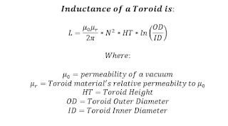
The basic formula for a toroidal inductor is:

The Fair-Rite paper uses log10 rather than natural log in its equation for inductance.  I would like to use this convention so that I can check my final derivation against Fair-Rite's formulas.  So, including this conversion, plus converting  permeability to H/mm (because the core dimensions are given by Fair-Rite in mm), I can express my final equation for inductance, as shown, below.


Note that ferrite's relative permeability is a complex value consisting of both real (μ') and imaginary (μ'') terms.  Here is an example of these values, versus frequency, for Mix 31, from Fair-Rite's "31-Material-Fair-Rite.csv" file (downloadable on this page):


Calculating Impedance:

The inductance equation, above, represents a complex inductance consisting of both real and imaginary parts.

The impedance of this inductor can be calculated by multiplying inductance by jω.  Note that ω (in radians/sec) can be replaced by 2π*frequency (where frequency is in Hz). 

The resulting impedance equation is shown, below.  I've also expanded the equation to show the series resistance and reactance components of this impedance. 


(Note that u'', the relative-permeability's imaginary component, determines the inductor's resistive losses, while u', the relative-permeability's real component, determines the inductor's reactance.)


Including Parasitic Capacitance:

But we are not finished.  I also need to include the effect of parasitic capacitance (e.g. inter-winding capacitance) on the overall impedance.  This capacitance can be modeled as a shunt capacitor in parallel with the inductor whose equation was defined, above, and its presence affects the inductor's self-resonant frequency (SRF):


Taking into account this parasitic capacitance, the actual impedance of the ferrite toroidal inductor is the calculated complex impedance of the inductor in parallel with the shunt capacitor's impedance:


If using MATLAB and its matrix-based math to calculate the actual impedance versus frequency, it is convenient to first convert impedance to admittance, sum these, and then convert the sum back to the actual impedance (matrix) of the device:


The section below is my MATLAB code for calculating the combined impedance of a ferrite toroidal inductor shunted with parasitic capacitance.

The code first reads the Fair-rite .csv file containing the ferrite relative-permeability data (versus frequency -- note that I modified the original file to shorten the frequency range to just those frequencies I am interested in).

Inductance is then calculated for both the Ferrite inductor and for the shunt parasitic capacitance.  These are then converted to admittances, summed, and then the sum inverted to give the actual impedance.

% Calculating Impedance of an Inductor wound on a Ferrite Toroid core.
% Date: 220209
% k6jca
%
% Inductance is calculated using a formula derived from equations in the
% paper: "Specifying a Ferrite for EMI Suppression," by Carole U. Parker
% of Fair-Rite Products.  This paper appeared in the June, 2008 issue of
% "Conformity", but should be found on the Fair-Rite site (Google title).
%
% Self-Resonant-Frequency (SRF) is simulated by specifying a shunt
% capacitance value paralleled with the inductor.
%
% The ferrite mix's u' and u'' values (vs frequency) come from a .CSV file
% downloaded from the Fair-Rite website.
%
% The inductor analyzed in this example is 12 turns wound on a Mix 31
% FT-240 core.
%
% Run on MATLAB Version R2020a


clear;
clc;
close all;

comment1='12 tight turns on FT-240 Mix 31 Core';  % for Plot annotation

% The ferrite mix u' and u'' data is in the following .CSV file.  Note that
% the data in Fair-rite's downloadable .CSV file spans the frequency range
% of 10 KHz to 1 GHz (much more than I need), and so I trimmed it down
% to cover only 1-60 MHz and renamed the file:
ftoread = '31-Material-Fair-Rite_1MHz-60MHz.csv'; % File with Mix data

N = 12;  % inductor's number of turns

% FT240 dimensions
OD = 61;    % outer-diameter, in mm
ID = 35.55; % inner-diameter, in mm
HT = 12.7;  % height, in mm

% Define the inductor's shunt capacitance (which affect the inductor's
% self-resonant-frequency (SRF).
% (One can manually adjust so that calculated SRF is similar to
% measured SRF).
Cp = 0.65e-12;               % in Farads
Cp_text = num2str(Cp*1e12);  % For plot annotation

% Read Fair-Rite's "mix" data from the CSV file and store in matrices.
% Note that the Excel file is in a directory parallel with the directory
% holding this matlab script.
A = readmatrix(['..\Excel\',ftoread]);  % CSV file is in EXCEL directory
f = A(:,1);      % frequency
u1 = A(:,2);     % Ferrite's u' value
u2 = A(:,3);     % Ferrite's u'' value

jw = 1i*2*pi*f;  % convert frequency to radians

% Calculate the inductor's impedance.
% (Formula derived from equations in the paper: "Specifying a Ferrite
%  for EMI Suppression," by Carole U. Parker of Fair-Rite Products.)
Zl = jw*4.6052e-10*(N^2).*(u1-1i*u2)*HT*log10(OD/ID);

% The shunt capacitance is in parallel with the inductor, and is
% the source of the inductor's Self-Resonant-Frequency.
%
% Because it is in parallel, a simple way to calculate its effect
% on impedance is to convert the inductor's and capacitor's impedances
% to admittances (admittance is just the inverse of impedance), add them,
% and then convert the sum back to impedance.
% MATLAB's 'RF Toolbox' has two nice routines for doing the matrix
% inversions: z2y() and y2z().
%
YZl = squeeze(z2y(Zl));         % inductor's admittance
YCp = (jw*Cp);                  % capacitor's admittance
Yactual = YZl + YCp;            % sum admittances
Zactual = squeeze(y2z(Yactual));% Final impedance (Z(inductor) paralleled
                                % with Z(cap)) is the inversion of Y

The MATLAB script can be downloaded from the following github directory:

https://github.com/k6jca/Calculating_Ferrite_Toroid_Inductor_Impedance

Note that the script in the directory contains the MATLAB code, above, plus code (not shown above) to generate the plot, below.

I ran my code using MATLAB revision R2020a, but you will need at least MATLAB revision R2019a (it's required for the readmatrix() function).  Of course, you can always use an earlier version, but you'll need to replace readmatrix() with something else.

The same caution applies to the sgtitle() function.  This function first appears in MATLAB revision R2018b.


Impedance of 12 turns on a Mix 31 FT-240 Ferrite Core:

Below are curves shown the calculated impedance of an inductor created by winding 12 turns around a Mix 31 FT-240 core.  Impedance is shown in terms of Magnitude and Phase, and also in terms of series Resistance and Reactance.

The shunt capacitance was set to a value of 0.65 pF.  (The next section explains why 0.65 pF was chosen.)


Selecting a Shunt Capacitance value:

Why choose 0.65 pF?  Why use any capacitance?

If there were no shunt capacitor (i.e. its capacitance = 0 pF), then there is no self-resonant point for this inductor (at least out to 60 MHz) -- the inductor remains inductive over the frequency range of 1 to 60 MHz:

But measurements made with a VNA exhibit a resonance.  

And so I chose a shunt capacitor value (in this case 0.65 pF) that makes the resonant frequency of the ferrite inductor's calculated impedance the same as the resonant frequency of the Y21-derived impedance (derived from the VNA measurements), as shown below (i.e. both the calculated phase and the impedance-from-Y21 phase cross 0 degrees at the same frequency).

As you can see, the calculated impedance, although not exactly the same as the impedance found via the Y21 method, is in the ballpark. Differences between calculated and measured impedances could be caused by any of a number of factors -- dimensional variations in core size, mix variations, actual winding style vs. ideal winding style, measurement error, etc.

(Note: also shown is the impedance measured using S11, which I consider to be an inferior method of measuring common-mode choke impedance.)


Conclusions and Notes:

1.  I consider the Y21 method of measuring a common-mode choke's impedance to be superior to the G3TXQ method of using only a VNA's S21 measurement, but, in the range of 1 to 30 MHz, the difference is not that significant (in my experience).

2.  The value of the parallel parasitic capacitance is a subjective choice.  I chose a value to make the resonant frequency of the calculated impedance the same as the resonant frequency of the Y21-derived impedance. But is this the best choice?  I do not know.

3.  If a multi-pole RLC ladder-network model is synthesized from the measured impedance (i.e. the Y21-derived impedance), and the capacitance of this synthesized model compared to the shunt capacitance I added to the Fair-Rite calculated inductance, the values are quite close (i.e. 0.62 pF for the synthesized model versus 0.65 pF for the Fair-Rite calculated Z).

The synthesized RLC ladder-network, created by Dick Benson, W1QG, using a custom MATLAB tool that will synthesize a network from the S-parameter measurements of an inductor (e.g. my VNA measurements for the 12-turns on the Mix 31 FT-240 core), looks like this:


You can see that the derived capacitance is 0.62 pF.  Quite close to the 0.65 pF I chose for the Fair-Rite derived model.

How accurate is this multi-pole synthesized RLC model to the Y21-derived measured impedance?  Comparing their plots below  (yellow = Y21-derived, cyan = synthesized), you can see that they are quite close.


My Balun (and 80-Meter Loop) posts:

I might have made a mistake in my designs, equations, schematics, models, etc.  If anything looks confusing or wrong to you, please feel free to comment below or send me an email.

Also, I will note:

This design and any associated information is distributed in the hope that it will be useful, but WITHOUT ANY WARRANTY; without even the implied warranty of MERCHANTABILITY or FITNESS FOR A PARTICULAR PURPOSE.

Thursday, January 20, 2022

Common-Mode Chokes: Removing Capacitance Effects from S11 Impedance Measurements

One way to verify the impedance of a common-mode choke (i.e. CM choke) is with a Vector Network Analyzer (VNA), such as the Agilent 8753 series or the popular nanoVNA.

Using such a VNA, a common mistake is to try to determine a CM choke's impedance using an S11 measurement -- this method of determining CM choke impedance can lead to very inaccurate results unless the user is aware of the potential pitfalls and how to correct for them.  (Determining CM choke impedance with an S21 measurement is usually a better method.)

An example of an erroneous S11 CM choke measurement is shown in the figure, below.  The choke consists of 12 turns around a Mix 33 FT-240 core.  (Note that this isn't actually a common-mode choke -- it is simply a choke, but its impedance would be the same as a common-mode choke wound the same way.)

The plot shows a maximum impedance of about 5600 ohms at 7 MHz, after which impedance falls off with frequency.  

But does this plot really represent the impedance of the choke?

If I use the G3TXQ S21 method of measuring a common-mode choke (this method is described here and here), the |Z| plot looks completely different, with a peak of 7400 ohms at 25 MHz:

Why the difference?  And can I modify my S11 measurement to give the same (or close to the same) results as the S21 measurement?


The Effect of External Capacitance:

A choke (common-mode or other type) is a two-terminal inductor that, when including its own parasitic capacitance and series resistance, can be modeled as shown in the figure, below:


To measure the device's impedance using a VNA S11 measurement, I connect it across Port 1 of the VNA.  But note that the test setup has different sources of parasitic capacitance.  

For example, there is the VNA port's intrinsic capacitance (i.e. internal port parasitic capacitance), as well as parasitic capacitance external to the VNA (caused by, for example, coupling between the DUT's leads, coupling of the DUT to the instrument (e.g. chassis ground), etc.).


The effect of the VNA's internal port capacitance upon the DUT measurement can be  removed by performing the normal VNA Short-Open-Load calibration.  Assuming that the Open calibration standard is close to a perfect Open (or that its imperfections have been programmed into the VNA, so that the VNA can compensate for them), then, following calibration, a 10 pF cap (for example) placed across the VNA's Port should measure to be 10 pF, despite the value of the VNA port's internal capacitances.


But the external parasitic capacitance is not removed by the VNA calibration process.  And this capacitance will change the self-resonant frequency of the DUT.  

In the case of my 12-turn choke on the mix 31 core, if I compare the S11 |Z| measurement to the S21 |Z| measurement, I see that the external parasitic capacitance has lowered the self-resonant frequency of the choke from 25 MHz to 7 MHz.  A significant change!  


Removing the Effect of the External Parasitic Capacitance:

We can remove the effect of the external parasitic capacitance from an S11 impedance measurement if we know (or can estimate) its capacitance value.

Per the figure, above, the impedance that is actually measured via S11 is:

   Z(S11) = Z(DUT) || Z(Cexternal) = 1/(1/Z(DUT) + 1/Z(Cexternal))

We can express this measurement in terms of admittances:

   Y(S11) = Y(DUT) + Y(Cexternal),

where:

   Y(DUT) = 1/Z(DUT) and Y(Cexternal) = jωCexternal

Rearranging the admittance equations:

   Y(DUT) = Y(S11) - Y(Cexternal)

and Z(DUT) is easily found by simply inverting Y(DUT):  Z(DUT) = 1/Y(DUT)

If I make the assumption that the external capacitance is around 2 pF (I'm going to use 1.95 pF for the plot, below) and calculate Z(DUT) per the following procedure, I get a "compensated" value of S11 impedance is now much closer to the S21 impedance measurement, as shown by the third line in the plot, below:


Why 1.95 pf?  I'll explain this in the next section, below.


R and X versus |Z|:

I'm really not interested in the magnitude of the impedance of a common-mode choke.  Although a high magnitude of impedance might seem great, it really tells me nothing about how the choke will behave when installed in an antenna system, because the choke's reactance (whose value is not known if we only examine the magnitude of the impedance) might actually worsen common-mode rejection.  (More on a CM choke worsening CM rejection here and here).

Unless you can characterize the impedance of common-mode paths of your antenna system, then measurement of the magnitude of Z (i.e. |Z|) is not very useful.

Instead, calculate the common-mode choke's resistance, as it is this component of the common-mode choke's impedance that is guaranteed to reduce common-mode currents, even if the choke's reactance happens to unfortunately series-resonate with, say, a coax-cable's common-mode path impedance.

For this reason, I always characterize a common-mode choke's impedance in terms of R and X, and I ignore |Z|.

The plot below shows the DUT's impedance converted into R and X for S11, S21, and the compensated S11 measurements:


Let's examine the plots, above, and get back to the question of why did I chose 1.95 pF for my shunt capacitance value...

Later in this post I will show that the shunt capacitance measures to be around 2 pF.  I don't know the exact value because the Y21 method I use to calculate shunt capacitance is a lumped-element approximation of what is actually a distributed circuit.  And, because this model is a circuit approximation, its values are also approximations.

I chose 1.95 pF because it gives R and X values that are fairly close (to my eye) to the R and X values found via the S21 method, as you can see in the plot, above.

If I make the capacitance value smaller, the peak of R will shift to the left, aligning it better with the peak found via S21, but the higher frequency values of R will fall further away from the values found via S21.

And if I increase C, those higher frequency values will align better, but the peaks move further apart.

So I chose 1.95 pF as a reasonable compromise.  The next section shows better how R and X vary with choice of shunt capacitance value.

Sensitivity of Z, R, and X to External Parasitic Capacitance:

How sensitive is the plot of the "compensated" S11 impedance measurement to the value of the external parasitic capacitance?

In addition to the original S11 and S21 |Z| plots, the figure below has three |Z| plots of the compensated S11 measurement using three different values of capacitance.  I've selected 2.0 pF as the "nominal" capacitance, with the other two capacitances being the this nominal capacitance varied by +/- 5% (i.e. 1.9 pF and 2.1 pF).  You can see that there is an appreciable change in |Z| at the higher frequencies. 


The figure below shows the R and X components for the original S21 plot as well as for the compensated S11 measurement using the two +/- 5% values of external capacitance (i.e. 1.9 and 2.1 pf).


Note that in this example, a change in capacitance of 10 % results in roughly a 20% change in the frequency of peak choke resistance!


Measuring Shunt Capacitance:

I can get an idea of the value of the parasitic shunt capacitance of my S21 Fixture by using the "Y21 method" to calculate three impedances of the fixture:  the series impedance between ports 1 and 2, and the shunt impedances (to ground) at either port.

To perform the S-parameter measurements for the Y21 calculations, I first perform a full 2-port VNA calibration in which the THRU standard is a short BNC barrel:


And then I replace this barrel with the "S21 Fixture" and measure the fixture's S-parameters:

The fixture's S-parameters, with shorting wire attached, are:

The figure below shows the fixture's series-impedance (displayed as R and X) as calculated using two methods: G3TXQ's S21 method and the Y21 method.

G3TXQ's method does not take into account the VNA port shunt impedances, which can result in errors, such as the resistance component of the series-impedance going negative, as shown in the next plot.  But if I use the Y21 method, I can model the measurement circuit as a three-element Pi network and calculate both the series impedance and the two shunt impedances:


Using the Y21 method we see that the fixture, when shorted with a wire, looks like a series impedance of 0.21 + jω200e-9 ohms (i.e. it is about 200 nH of inductance in series with about 0.2 ohms of resistance):

And the shunt capacitances at either port are about 2.1 pF:

Note that these shunt capacitances are modeled as lumped-elements, approximating what is actually happening with the fixture's distributed circuit.


Impedance Measurement using the Y21 Method:

Let's use the Y21 method and calculate the series and shunt impedances when my 12-turn choke is connected to the S21 fixture.

The figure below shows R and X for the choke as calculated from S11, S21, S11 compensated for external port capacitance (1.95 pF), and the Y21 method. 


The figure below shows the external shunt capacitance values calculated with the Y21 method.  Note that these are now closer to 3 pF, rather than 2 pF.  This is possibly due to distributed coupling from the physical structure of the choke to ground, which then becomes part of the 3-component lumped-element Y21 circuit approximation.


Conclusions:

1.  Stray shunt capacitance can greatly affect the measured impedance of a common-mode choke if measuring it using a VNA's S11 measurement.  If you know the approximate value of your stray shunt capacitance, you can remove its effect from the measurement by converting impedances to admittances, and then subtracting from the measured admittance the admittance of the stray shunt capacitance.

But if you do not have a reasonable idea of what your stray capacitance value is, your results might not represent the choke's actual impedance.

And this is exactly the problem with the S11 method of measuring common-mode choke impedances -- what is the shunt capacitance?

2.  G3TXQ's S21 measurement method provides a better measure of common-mode choke impedance than S11 measurements.  But the Y21 method of measuring impedance (from an S21 measurement) is superior to G3TXQ's method.


My Balun (and 80-Meter Loop) posts:


Standard Caveat:

I might have made a mistake in my designs, equations, schematics, models, etc.  If anything looks confusing or wrong to you, please feel free to comment below or send me an email.

Also, I will note:

This design and any associated information is distributed in the hope that it will be useful, but WITHOUT ANY WARRANTY; without even the implied warranty of MERCHANTABILITY or FITNESS FOR A PARTICULAR PURPOSE.