Tuesday, April 12, 2022

Repair Log: HP 3314A, Part 2

This post is part 2 of my HP 3314A Function Generator troubleshooting posts, in which I continue troubleshooting my swap-meet find.  

Part 1 is here.


Battery Replacement:

The HP 3314A contains a Lithium battery to keep power applied to the CMOS RAMs (U211 and U212) and to the Reset Circuitry (U203, an MC14584B Hex Schmitt Trigger IC) when the 3314A is powered off.

 The image below shows the dead battery that was in the 3314A when I purchased it.  Although not easily seen in the picture below, there are two wires attached to the PCB that are pushed against the ends of the battery, but they are not soldered to it.  So electrical contact with the battery's terminals depends upon the physical pressure of the two wires against the battery's ends. 

My guess is that the two wires attached to the PCB wereleads that were part of an older, originally installed by HP, battery, and a previous owner simply clipped these two leads from the ends of that original battery and then pressed them against the terminals of a modern replacement battery that did not have wires attached to it, hoping that this physical contact would provide a reliable electrical contact.

I purchased a CR123A battery holder and new 123-style Lithium 3 volt battery via Amazon and, after removing the original two wires on the board, I used two new wires to connect the holder to the PCB.  This assembly is held in place with a tie-wrap.


ROM Failure:

Even with the bad CMOS RAM temporarily replaced (see Part 1), the unit would still end up with a blank seven-segment display after the power-up count-down sequence.  Why was the microprocessor failing to continue?

Perhaps there's another memory failure.

Fortunately, HP included a number of self-tests in the HP 3314A.  One of these is a memory test, which verifies the contents of the ROM memory (of which there are six ROMs in my early version of the 3314A (U207-U210, U236, U238)), as well as the RAM (U233, U234) and CMOS RAM (U211, U212; these last two being the battery backed-up RAM).

This memory test can be invoked by holding down the ARB button while turning on the 3314A.  It can take 20 to 30 seconds to complete, and, when finished, it will display which memory devices test GOOD by turning ON a front-panel LED for each good device.  If the associated LED is OFF, then the memory device failed the test.


When I invoked this test, the AMPLITUDE LED remained OFF, signifying that U236 was bad.

(Note -- when I first tried to invoke this test, prior to replacing U212 (the bad CMOS RAM IC), all of the LEDs would turn OFF and the test would never finish.)

Pinout-wise, the six on-board ROMs seem equivalent to 2364 ROMs.  These are 8Kx8 bit memories.  I have 2764 EPROMs in my junk box (from designs I did 40 years ago) that are also 8Kx8 devices.  Could I program one of my EPROMs to replace the bad on-board ROM?

But first, were the 3314A ROM binary files even available?  

A query to the HP/Agilent/Keysight groups.io site (https://groups.io/g/HP-Agilent-Keysight-equipment) quickly got a reply to take a look at the Ko4BB web-site, which has files for both the early version of the 3314A (like mine) which had six 8Kx8 ROMs, and the later revision which had a single 64Kx8 ROM.

So binary files were available, but one more issue remained -- the original ROMs were 24 pin devices, but the 2764 EPROM is a 28 pin device.

I could wire up an adapter board, myself, but fortunately, one can purchase adapter boards for this purpose, and eBay had just the thing.  (Apparently this was a common modification for the Commodore computer -- search for "2364 EPROM Adapter").

Here's a photo of the adapter kit I purchased from eBay (this photo is from the eBay listing):


Note that pin 27 of the 2764 EPROM (its /PGM pin) should be tied to VCC for normal READ operations.  This pin is not normally tied high on the adapter board, but the board does include pads to accomplish this -- I simply applied a solder-short from the "A14" pad to the "VCC" pad (these pads are visible in the center of the board in the image, above).

Pin 26 of the 2764 EPROM should remain floating (No Connection).  Note that this pin corresponds to the "A13" pad on the adapter board, and it should remain unconnected.

With the adapter built and an EPROM programmed (using an inexpensive TL866A PROM Programmer, available, for example, via Amazon), I soldered the adapter to the PCB in place of the original ROM and inserted the programmed PROM into its socket.


I powered up and...hurray!  The seven-segment display did not blank out after the initial count-down following power up!  

And when I invoked the Memory Test at power-up, all memories passed.

But there were still problems -- now the unit displayed the following errors during its power-on calibration procedure:

E30 (No Frequency Detected)

E34 (Signal Amplitude Outside Measurement Range)

So on to the next problem...


Error E30:  No Frequency Detected:

The Service Manual has a flowchart for troubleshooting Frequency Calibration errors.  Following this chart led me to the box labeled "Common Mode Rejection Circuitry":


The Common Mode Rejection Circuitry is part of the "Triangle Integrator" schematic, below.  The purpose of this circuitry is to keep the DC level at the Source Pins of Q220 (i.e. pins 1 and 5) at about -5 Vdc.  

On my board I measured the "Common Mode Sense" voltage (at the base of Q211) to be -3.4 volts, not the specified -5 volts.  Clearly there was a problem.  But was the problem actually with the common-mode circuitry, or was it somewhere else, with the symptoms exhibiting themselves as a common-mode problem?


(Important Sidebar Note:  Although the Service Manual shows voltages at Q220 pins 1 and 5 having a DC offset of -5 Vdc (Waveform 1, Figure 8-15, although good luck discerning this level from the manual download from the Kesight site), these two voltages can actually be a bit lower than -5 Vdc (e.g. -5.4 Vdc), due to Q211 base current, even if the "Common Mode Sense" signal at the base of Q211 is -5 Vdc)).

But back to the problem -- why was the Common Mode Sense level so far off?

First, I needed to understand the circuit, starting with the Triangle Integrator circuitry.  

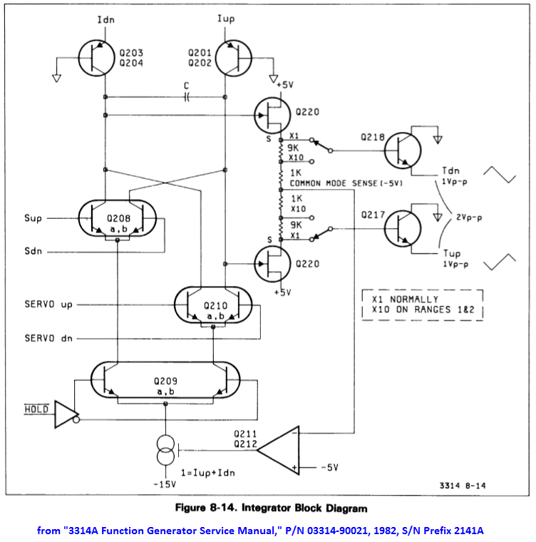
The functional operation of the Triangle-wave generator can be understood using the block diagram, below.  


First, note that in normal operation (e.g. the generator's state after power-up), the path through the Q210 differential pair is not used.  Instead, Q208 controls the generation of the triangle wave.

Basically, a constant current is passed through the capacitor C (connected across the collectors of the two differential pairs Q208 and Q210), first charging the capacitor in one direction (Iup and Idn both passing through, for example, the left-hand transistor of the differential pair, Q208a, with Iup charging the capacitor).

A downstream comparator (not shown in the block diagram, above), monitors the voltage across the capacitor and, when this voltage reaches a threshold, it flips the states of the Sup and Sdn control signals, forcing the capacitor to charge in the opposite  direction (i.e. via Idn, with both Iup and Idn now passing through Q208b).

If everything is working properly, this flipping back and forth of the charging path should result in a 1 volt peak-to-peak triangle waveform at the output of the Triangle Integrator circuitry (i.e. 1 Vpp at the emitter of Q217 and 1 Vpp at the emitter of Q218).  And because Q217 and Q218 are emitter followers) the same peak-to-peak levels should be seen at each of Q220's two Source pins (pins 1 and 5).  

But when I measured the signals at  Q220's Source pins, there wasn't a 1 Vpp signal present on either pin. Instead, one Source pin (pin 1) was stuck at 0.7 Vdc, while the other Source pin (pin 5) was sitting at -7.5 volts.


The voltage delta between these two pins was 8.2 Vdc (much greater than the 1 volt delta it should have been).  And it was because of this excessive voltage delta that the Common Mode Sense voltage measured to be -3.4 Vdc and not the desired -5 Vdc (the Common-Mode Sense voltage, assuming that Q211's base current is insignificant, is a function of the voltage divider consisting of  R233, R234, R237, and R23 connected in series between the two Source pins of Q220, and thus this voltage should equal the average of the voltage between these two pins (i.e. (0.7 + (-7.5))/2 = -3.4 V).

So why was the voltage delta between the two source pins so large?  And why weren't the transistors in the Q208 differential pair flipping  back and forth to create the triangle wave?  Was there a problem with the triangle generator, or maybe the comparator?

This was looking a lot less like an issue with the Common Mode Rejection circuitry and instead an issue somewhere else.

Probing the circuit's transistor voltages gave me some very strange results when I looked at transistor voltages in aggregate, but after digging a bit further I found that my confusion was, in fact, caused by a schematic error in which the transistor reference designators for Q208a and Q208b were swapped, compared to the labels on the PCB silkscreen.  The correct reference designators are shown, below:


With that schematic issue resolved, the measured Integrator's voltages now made sense, and the problem would seem to be further downstream, at the comparator.  (It is the comparator that flips the Sup and Sdn signals back and forth, which in turn control the charging direction of the integrating capacitor via Q208a or Q208b).

While troubleshooting the comparator's voltages I ran into another documentation error -- this time in the Comparator Block Diagram:


(And although it is not shown in this blog post, Figure 8-19 has the same pin errors.)

As I probed the DC voltages of U303 (a CA3102 dual differential amplifier IC) it quickly became apparent that something was really messed up.  For example, the device's Substrate pin (pin 5) was sitting at -4 Vdc instead of -15 Vdc.  The substrate pins voltage should be the lowest voltage on the chip, and it clearly was not (see the voltages in the image, below).


Also, the current into pin 11 (transistor base current) was a whopping 33 mA!

It looked like U303 was bad, but I didn't have any replacements in my junkbox.  Fortunately, I found some on eBay and ordered a couple.  But in the meantime I decided to make a simple replacement for the CA3102 using six discrete 2N3904 transistors to replicate the CA3102's two differential amplifiers.  It wouldn't be perfect -- the 2N3904 transistors weren't matched and their fT is much lower than that of the CA3102's transistors, but hopefully I could continue with my troubleshooting while awaiting the arrival of the CA3102 devices.

(Sidebar:  Interestingly, the CA3102 was already mounted in a socket.  I don't know if HP did this during manufacturing, or if someone later modified the board and added the socket.  If the former, maybe the CA3102 devices needed to be hand-selected to get the required performance.)

Below is an image of my "Temporary CA3102" replacement, using six 2N3904 transistors and built onto a 14-pin DIP header that, in turn, is plugged into a 14-pin socket at U303's location on the PCB:


With this temporary replacement installed on the PCB, there were no longer any "E30" errors at power up, and there was now a sine wave present at the 3314A's output!

But, even though there was now a sine wave output, there were still errors displayed at power up.  These errors consisted of one E31 error (frequency error exceeds correction capability) and four E34 errors (signal amplitude outside measurement range) that were displayed during the calibration sequence.

So on to the next problem...


Error E34:  Signal Amplitude Outside Measurement Range:

Error E34 identifies the signal amplitude as being "outside measurement range."  But what is "outside measurement range"?  

Unfortunately, the Service Manual seems to be mute on this error condition, but, if I measured the 3314A's output (across a 50 ohm load) with the 3314A's amplitude set to 1.00 volts (peak-to-peak) and 0 volts DC offset, the output level and offset were clearly not what they should have been, as the image below shows:


With the output amplitude set to 1.00 volts and no DC offset, the voltage across a 50 ohm load  measured to be 0.88 Vpp with an offset of -0.24 Vdc, not the desired 1.0 Vpp with 0 Vdc offset.  

Clearly there was a problem.

Because E34 is an "Amplitude Calibration" error, I decided to follow the Service Manual's "Amplitude Calibration Troubleshooting Flowchart" (figure 8-11B).

Following its flow and making the recommended measurements at the appropriate steps, I arrived at its conclusion that, "Maybe U502 or associated cells/circuits" were at fault.


Well, that's pretty vague.

And what is U502?  It is HP's custom "Sine Shaper" IC that converts the triangle wave into a reasonable facsimile of a sine wave.  If this part were bad, then I might as well abandon the project, because it was sure to be "unobtanium."

But it was too early to abandon hope, so I started troubleshooting by first examining U502's signals.

Well, U502's signals "seemed" good, in the sense that nothing was obviously out of whack, but there wasn't much information in the Service Manual as to what U502's signals should actually look like.

Assuming (hopefully) that U502 wasn't the issue, could the problem be in an earlier stage?  For example, I had noticed that the DC levels at the Integrator circuit's Q220 Source pins were about 0.4 volts lower than the image for the waveforms shown in the Service Manual (i.e. they measured at -5.4 volts instead of -5 volts), as shown, below:


Could this offset be the problem?  A quick test (raising the Source voltages of Q220 from -5.4 to -5 volts by paralleling R219 (in the Q211, Q212 circuit) with a variable resistor) showed that changing this DC offset had absolutely no effect on the 3314A's output voltage level or offset.

Hmmm, could the problem be in the next stage, the Transconductance Amplifier?

Did not seem so.  DC voltages seemed reasonable, and signal levels at the bases of Q203 were correct.

So the signals going to the Sine Shaper seemed to be reasonable, at least as far as I could determine (which was not very far).

Again, hoping that the Sine Shaper IC was not the issue, perhaps the problem was in a stage following it.

The Sine Shaper drives the "Preamplifier" Stage (Figure 8-23 in the Service Manual), which in turn drives the "Output Amplifier and Step Attenuator" stage, whose output, in turn, goes to the output connector on the front panel.

As I measured the DC levels of the Preamplifier from input to output, they looked OK...but wait!  The node common to R611, R612, R606, R607, and R608 measured at 0 Vdc (which makes sense, as this should be the DC level of a balanced amplifier when there is no DC offset), but the DC voltage at the other side of R607 (i.e. at connector J1 to the Output Amplifier's input) was at -0.24 volts.


What happens to the DC level at the Preamplifier's J1 connector if I disconnect the cable between J1 and the input to the Output Amplifier?  The DC voltage at the output side of R607 goes to 0 Vdc, and the sine wave amplitude increases such that, when this point is terminated with 50 ohms, its amplitude is correct.  

That is, with the Preamplifier's output disconnected from the input of the "Output Amplifier" stage, and with the 3314A's amplitude set to 1 Vpp and 0 Vdc offset, the sine wave at the Preamplifier Output (terminated with 50 ohms) correctly measures to be 1 Vpp with 0 Vdc offset, instead of the 0.88 Vpp with -0.24 Vdc offset that would have been measured at the output of the Output Amplifier.

So the Output Amplifier would seem to the be culprit!  Here is an image of that board:


While probing the Output Amplifier's DC voltages, it quickly became apparent that Q10 was bad (an MPSH10 NPN transistor -- its Vbe measured to be 3.7 V).


I replaced Q10 and powered up the unit.  Success!  There were no longer any E34 errors during power-on calibration.


Important Note:  The scanned copy of the schematic for the "Output Amplifier and Step Attenuator" board in the downloadable Service Manual on the Keysight site (see Resource list, below) is missing some circuitry, which I've shown in the image, below (copied from a later manual revision):


Conclusion:

With all fixes installed, the 3314A's Calibration Sequence (initiated at power-up) successfully completes with no displayed errors.  And it plays the Hallelujah Chorus! (See here for an example).

I have not done any of the Performance Tests listed in the Service Manual.  I might do these at some future date, at which point, if there are any issues that need repair, there might be a Part 3 added to this 3314A troubleshooting series.

Finally, note that all troubleshooting was done without the benefit of a Signature Analyzer.  However, if there had been problems with the digital logic, a Signature Analyzer (e.g. HP 5004A) would have been invaluable.


Other Notes and Comments:

1.  E31 Error:

The E31 error (that began appearing during the Power-up Cal sequence after I had replaced the bad U303 (CA3102) with my temporary "six 2N3904" replacement), disappeared when I replaced the U303 temporary fix with an actual CA3102 device.

2.  Replacing the CMOS RAM with higher-current devices:

If uPD444 CMOS RAMs are not available for replacing U211 and/or U212, other 1Kx4 devices can be used, if they are pin compatible.  Note, though, that if the new RAMs require higher Vcc current, then to prevent battery drain their power pins should not be attached to their respective pin 18 PCB pads (which are powered by the battery when AC power is OFF).     

Instead, lift the power pins (pin 18) of the two devices and connect these two lifted pins to +5 Vdc at the "front-panel" side of C17, as shown in the image, below (the example, below, uses two Intel D2148H RAMs in lieu of the two original NEC uPD444 RAMs):

With this modification, the CMOS RAM will no longer retain stored information when the 3314A is turned off.  And thus there will be an "E09" error (non-volatile memory lost; battery down), displayed at the end of the Power-up calibration sequence, every time the 3314A is powered up.


Resources:

HP 3314A Manuals:  https://www.keysight.com/us/en/support/3314A/programmable-function-generator.html

HP 3314A Repair in 3 parts:  https://diysquared.blogspot.com/2021/04/fixing-hp-3314a-function-generator-part.html

HP 3314A Repair on YouTube:  https://www.youtube.com/watch?v=wNxgBubSfH8

HP 3314A Repair (on Antique Radios forum):  https://antiqueradios.com/forums/viewtopic.php?f=8&t=360491

HP 3314A Teardown (EEVblog):  https://www.eevblog.com/forum/testgear/hp-3314a-function-generator-teardown-explanation/

HP 3314A Playing the Hallelujah Chorus:  https://www.youtube.com/watch?v=H90d6sPUF6A
(Note:  Hold down FUNCTION (the blue key), SW/TR INTVL, and START FREQ while powering up the unit).

HP 3314A ROM Images:  http://www.ko4bb.com/getsimple/index.php?id=manuals&dir=01_ROM_Images_and_Drivers/HP_3314A_Eprom


Standard Caveat:

As always, I might have made a mistake in my equations, assumptions, drawings, or interpretations.  If you see anything you believe to be in error or if anything is confusing, please feel free to contact me or comment below.

And so I should add -- this information is distributed in the hope that it will be useful, but WITHOUT ANY WARRANTY; without even the implied warranty of MERCHANTABILITY or FITNESS FOR A PARTICULAR PURPOSE.

Tuesday, March 29, 2022

Repair Log: HP 3314A, Part 1


At a recent swap-meet I came across an HP 3314A Programmable Function Generator that was described as non-operational but was physically in good shape.

In my opinion, HP cases make great project boxes (see here, here, and here), and this case looked like it would be an excellent case for a future, yet-to-be-defined project.

And so I made an offer based solely on the idea of scrapping the 3314A's electronics but keeping its case and internal chassis.  The offer was accepted, and the 3314A came home with me.

But after I had returned home, I had second thoughts about my plan to scrap the unit.  Why not try to fix it, if that were possible?

And thus this blog post, which describes my efforts to bring this HP 3314A back to life.


Initial Power-On Error:

The first problem I came across was at power-up -- the unit would cycle through its initial count-down following power-up, and then it would hang.  The count numbers displayed during the Power-up cycle would often also be screwed up.  And at the end of this cycle, sometimes the 3314A would hang with the LED numerical display being blank, and sometimes the display would show Error Codes E13 or E43.

Looking in the manual (section 3-1), Error Code E13 does not exist, and, although Error Code E43 exists, it is an HP-IB Error Code meaning "Invalid Data."  Given that the instrument was not in Remote mode (i.e. HP-IB mode), the display of this last error code could be meaningless and a result of some other error.

Note that immediately following power-up, the unit's 3-digit numerical display should show the following sequential count-down:

999
888
777
666
555
444
333
222
111
000

The video, below, demonstrates the Count-down problem:

You can see from the video that the displays are changing, so the 3314A is attempting this count-down, but the digits of the first counts are screwed up.

But before I go any further...

A quick note on my initial trouble-shooting:

The HP Service Manual (downloadable from the Keysight website: HP 3314A Manuals) recommends trouble-shooting using Signature Analysis.  Unfortunately, I was at my wife's place in Nevada City, CA, at the time of this initial trouble-shooting, and my Signature Analyzer was back at my house in Silicon Valley, CA.

(Plus, the SA unit has been sitting in a box, untested, for at least 20 years (another swap-meet find), and I had no idea if it worked, or not, as I've never had a need to use it!)

So, this initial phase of trouble-shooting was done with a 2-channel oscilloscope...


Probing the Front Panel Assembly:

Because segments of the LED seven-segment displays were either being incorrectly kept off or, alternately, incorrectly illuminated, it made sense to start my trouble-shooting at the Keyboard assembly where the seven-segment displays reside.

But I immediately encountered several issues.  The first issue is that the HP schematic has a number of errors.

The image, below, shows my corrections, in red.  You can see that U1's (74LS273) inputs were incorrectly assigned.  Also, the pin number of the LED displays are incorrect.

Here's a closeup of U1.  Its correct pin number assignments are shown in red:

And here's a closeup of the correct seven-segment display pinout (in red):

(Note that I also corrected the names of the three signals driving the common-cathode pins of these three displays to match the net names assigned to their respective drivers.)

The image below shows the correct pin number (in red) and the associated data bit from the 8-bit bus (in blue) for each segment of the LED.

When count-down sequence first starts, the first count presented on each seven-segment display is '9', and then this number counts down (8, 7, 6, etc.).  The numbers are the same on all three seven-segment displays, so the displayed numbers should be, in sequence, 999, 888, 777, 666, 555, etc.

Thus, the segments of the seven-segment display associated with data-bits DL0, DL1, DL2, and DL3 should be ON for the first count-down digits (9, 8, 7...), but, as you can see in the video, above, they are OFF.  These will later turn ON for lower counts (e.g. 3, 2, 1, 0), but at the start of count-down they are OFF.

The image below shows the problematic segments (highlighted in yellow):


The Keyboard assembly is a multiplexed system with the segments of the seven-segment displays sharing the same "row" signals (as in a row-column matrix) as the other front-panel LEDs.  Thus, probing a segment to see if it is correctly turning on or off can be a bit of a challenge with a two-channel scope, especially with the count-down's count quickly changing as it counts down.

But by observing U1's outputs (the 'LS273) responsible for driving the numerical segments immediately after power-on, it was clear that U1's outputs were not being set to the correct state to drive these segments ON for the first few counts (a U1 output bit must be set LOW to turn ON a segment).

Tracing this failure back...the data at U1's inputs, arriving at the Keyboard from the Controller Board,  was also in the incorrect state for these counts.  Thus, U1 was simply passing on incorrect data from the Controller Board.

So time to move the probing to the Controller Board...


Probing the Controller Board:

At the controller board I started at the processor, looking at its Data Bus while triggering the scope on the rising edge of the clock clocking data into the U1 register on the Keyboard assembly.  This probing showed that the data from the microprocessor that was being written to the Keyboard assembly was also incorrect.

So why was the processor writing incorrect data?  Was it getting bad data from the PROMs (of which there are six)?  Or was RAM bad?  Or was something fighting the bus when the processor was attempting to read or write this data?

Even though I did not have a Signature Analyzer, I decided to invoke one of its tests (SA Test #1, in which switches 1, 2, 7, and 8 are turned ON), because I assumed this test would sequentially count through all of the microprocessor's addresses and I could look for errors either on the Address Bus or on the Data Bus during this time.

Everything was looking good until I got to the CMOS SRAM, U211 and U212 (NEC UPD444/6514 1Kx4 bit CMOS RAM).  The four data I/O pins of U212 had flaky looking levels for some of its read cycles.  Plus, these flaky levels would change with time.  

The image below (lower scope trace) shows the levels one of these pins (pin 11, or I/O4).  U212's outputs are enabled whenever the upper trace is low.


Compared to U212, the I/O pins of U211 looked fine -- it was only U212's four data pins that had the issue.  And these four data bits correspond to the low-order four bits of the Data Bus, which were the problem bits driving the Keyboard's seven-segment displays.

Could a bad U212 be the culprit?  I placed an order of a pair of new NEC UPD444 RAMs on eBay, but while waiting for them to arrive I thought I'd continue testing...

By the way -- the HP manual has some errors regarding SRAM power on the Controller Board.  My corrections are shown, below, in red:


Excessive Battery Current Drain:

After ordering replacement UPD444 CMOS SRAM from eBay, I decided to look around a bit more and see what other problems I could find while waiting for the SRAM to arrive.

One issue I had noticed when I first opened up the unit was that the battery backup was dead (the battery was sitting at about 0.45 volts), yet it was a fairly new battery (with a 2023 date).  Could it have been killed by excessive current draw?

Note that this battery serves two purposes:

First, it keeps power applied to U203 of the RESET circuitry (CMOS inverters), even when power is OFF, so that the RESET line can be properly driven when power is first applied.

Second, the battery provides power to U211 and U212 (the CMOS SRAM), to maintain the contents in these two SRAM chips even when the unit is powered OFF.

Per section 5.2 of the manual, battery current drain when power was off should be on the order of 1.35 uA (typical) to 18.5 uA (max), when measured as an equivalent voltage drop across R13, a 1K ohm resistor -- e.g. 1.35 uA of current would equal 1.35 mV across R13).

Replacing the dead battery with a bench supply set to 3.0 volts, I measured 0.495 volts across R13 -- in other words, current draw was 495 uA, not the spec'd 18.5 uA max!

No wonder the battery was dead!

The battery-power circuit is fairly simple, which means there weren't many suspects.  And because U212 (one of the two CMOS SRAMS) was on my "hit-list" of suspected bad parts, I decided to clip its VCC pin (pin 18) and see what happened to battery current.  

With the pin clipped (i.e. no VCC applied to U212), the voltage across R13 dropped way down (below the level that my Fluke DVM can measure) -- clearly U212 was the culprit!  


U212 Temporary Replacement Test:

OK -- two different tests pointed to U212 being bad.  Was there some way that I could verify this while waiting for my eBay UPD444 CMOS RAM to arrive?

A friend gave me a National MM2114N-L 1Kx4 bit RAM from his junk box.  This device draws more supply current than the original NEC part, so it would not be a satisfactory permanent replacement for the UPD444, but I thought I would give it a try to test my theory that it was U212 that caused the count-down errors.

So I removed the original part, installed an 18-pin socket in its place, and inserted the '2114 in its place (also, the battery had been removed, too (it was dead) -- if the battery had been good, though, the MM2114N would have presented a much larger than expected current drain, and I would have removed it before doing this test).

I turned power on, and...nothing.  The seven-segment displays remained dark!

Probing with the scope, I quickly discovered that with power ON, Vcc at the '2114 was around 3 volts, not the expected 5 volts.  

Power to the CMOS RAM is a diode-OR'd combination of Vcc (via CR2, when the unit is powered up) or the Battery voltage (via CR3, when the unit is powered down and the CMOS RAM thus battery-powered).

There is a 49.9 ohm resistor (R17) in series with CR2.  The Vcc current of the '2114 RAM was enough to create a significant voltage drop across this 49.9 ohm resistor.

The obvious temporary solution was to short out the resistor for this test, which I did.


Powered the unit back ON, and the count-down was now correct!  Therefore, the count-down problem was caused by a bad U212 CMOS RAM IC.

Here's a video of the correct power-up countdown, with the MM2114N-L as the temporary replacement for U212:


Even thought the count-down is now correct, the unit still fails at the end of the count-down, either by blanking the seven-segment displays (as shown in the video, above) or showing (sometimes briefly) the two error codes mentioned above.


(An interesting question (unanswered) is why did HP add R17 in series with CR2?  My guess is that it has to do with current-limiting CR2's current at power-up, but why?  Note, its P/N is 1902-0535.  With 50 ohms in series and assuming a direct short from CR2's cathode to ground at power-up, CR2's initial current surge would be around 100 mA. Is the Schottky diode that sensitive to a temporary current surge?).


More Troubleshooting continues in Part 2!


Other Manual Issues:

Another Keyboard schematic error:  There are no net names assigned to the inputs of the four U5 drivers ('LS05 devices), so it is impossible to tell which output they actually connect to.


Resources:

HP 3314A Manuals:  https://www.keysight.com/us/en/support/3314A/programmable-function-generator.html

HP 3314A Repair in 3 parts:  https://diysquared.blogspot.com/2021/04/fixing-hp-3314a-function-generator-part.html

HP 3314A Repair on YouTube:  https://www.youtube.com/watch?v=wNxgBubSfH8

HP 3314A Repair (on Antique Radios forum):  https://antiqueradios.com/forums/viewtopic.php?f=8&t=360491

HP 3314A Teardown (EEVblog):  https://www.eevblog.com/forum/testgear/hp-3314a-function-generator-teardown-explanation/

HP 3314A Playing the Hallelujah Chorus:  https://www.youtube.com/watch?v=H90d6sPUF6A
(Note:  Hold down FUNCTION (the blue key), SW/TR INTVL, and START FREQ while powering up the unit).

HP 3314A ROM Images:  http://www.ko4bb.com/getsimple/index.php?id=manuals&dir=01_ROM_Images_and_Drivers/HP_3314A_Eprom


Standard Caveat:

As always, I might have made a mistake in my equations, assumptions, drawings, or interpretations.  If you see anything you believe to be in error or if anything is confusing, please feel free to contact me or comment below.

And so I should add -- this information is distributed in the hope that it will be useful, but WITHOUT ANY WARRANTY; without even the implied warranty of MERCHANTABILITY or FITNESS FOR A PARTICULAR PURPOSE.

Monday, March 21, 2022

Representing a Transmission Line as a 2-Port Network

In this blog post I will derive equations representing a transmission line of characteristic impedance Zo and of length 'l' as a two-port network.  As a result, there will be a total of four different pairs of equations, each pair representing the two-port network in a different way.

These pairs of equation will be:

1.  V and I at Port 2, in terms of V and I at Port 1, for a lossy transmission line.

2.  V and I at Port 1, in terms of V and I at Port 2, for a lossy transmission line.

3.  V and I at Port 2, in terms of V and I at Port 1, for a lossless transmission line.

4. V and I at Port 1, in terms of V and I at Port 2, for a lossless transmission line.

(These last two sets of equations are special cases of the first two sets).

The image below shows these voltages and currents for both the transmission line and its two-port model.


The first two sets of equations that will be derived are summarized by the two matrix equations, below:


To derive the two equations in the first set of these equations, let's start with some fundamental definitions...

 
Some fundamentals:

Assume that the transmission line has on it both a forward voltage wave (traveling from left to right) and an independent reverse voltage wave (traveling from right to left).  At any point on the transmission line these forward and reverse voltage waves create forward and reverse current waves:


If we were to measure the voltage at any point on the line, the voltage we would measure at that point will be the sum of the forward voltage and the reverse voltage at that point.  

Note that the forward voltage and the reverse voltage each has its own amplitude and phase at that point.

Similarly, the current at that point will be the difference between the forward current and the reverse current (because the currents are flowing in opposite directions). 


Recognize that for either the forward wave or the reflected wave, their voltage and currents follow ohms law, independently of the other wave (because of the Principle of Superposition).  E.g. I+ = V+/Zo and I-=V-/Zo, where Zo is the transmission line's characteristic impedance.

So we can write equations for the Total Voltage and Current at each end of the transmission line in terms of the forward and reverse voltages at those points:

We can also express the forward and reverse voltages at either end of the transmission line as functions of the Total Voltage and Current at either end:

I will use equations 1, 2, 3, and 4 (in the figure, above) to derive the two-port network equations, but before I go any further in this derivation, let me first define a transmission line's "Propagation Constant."


Sidebar on the exponential terms e-γl and eγl :

Assuming a sinusoidal signal on the transmission line, the exponential term e-γl  (or eγl) represents the effect on a sine wave's amplitude and phase, due to the transmission line's Propagation Constant, γ, as that wave travels along the transmission line.

The other variable in the exponent is 'l', which represents the length that the wave has traveled (or will travel) along the transmission line.

The Propagation Constant is a complex number: γ = α + jβ, where α represents a "real" change in signal amplitude (either positive or negative, i.e. attenuation or gain), and jβ represents a phase shift of the sinusoidal signal, either a positive phase shift or a negative phase shift.  

Both of these values are in terms of unit-length, and so when substituted into the exponential, multiplying α by the length of the line gives overall attenuation (or gain, depending upon reference point), and multiplying jβ by length gives phase-shift for the wave's journey along a defined length of line.

If we were to take a snapshot in time and simultaneously compare the Forward Voltage V+ at point 1 with the Forward Voltage V+ at point 2, we would see that the voltage at point 2 has a negative phase shift compared to the phase of  V+ at point 1, because the voltage at point 2 represents an earlier version of  V+ that had been at point 1 at an earlier point in time, compared to the V+ that is currently at Point 1. 

We would also see that the amplitude of V+ at point 2 has been attenuated relative to its original amplitude at point 1 due to transmission line loss as it traveled from left to right along the line.   Thus, γ's "α" term (in the Propagation Constant's equation  γ = α + jβ) is negative to represent this loss at point 2 compared to the amplitude at point 1.

The figure below demonstrates both the attenuation and the phase shift at point 2, compared to point 1, for the Forward moving voltage wave:


With the same "snapshot in time," we can also simultaneously compare the Reverse Voltage V- at point 1 with the Reverse Voltage V- at point 2.  

We would see that the voltage at point 2 has a positive phase shift compared to the phase of  V- at point 1, because the voltage at point 2 represents a later version of V-  that has yet to arrive at point 1, compared to the phase of V- that is currently at Point 1. 

We would also see that the amplitude of V- at point 2 has not yet been attenuated compared to the amplitude of V- at point 1, because it has not yet traveled from right-to-left along the line, and thus it has not yet been attenuated by line loss.  Therefore, γ's "α" term (in the Propagation Constant equation  γ = α + jβ) is positive for V- at point 2 , not negative, because the amplitude at point 2 is larger compared to the amplitude at point 1.

The figure below demonstrates both the amplitude and phase at point 2, compared to point 1, for the Reverse moving voltage wave.:

With this information and the equations, above, we can derive network equations that represent a lossy transmission line of length 'l'.


Lossy Transmission Line Equations for V2 and I2 in terms of V1 and I1:

From the previous two figures that describe phase-shift and attenuation of V+ and V- at Point 2 compared to our reference at Point 1, we can create the identities represented by equations 5 and 6 in the figure, below, and, using these, represent V2 as a function of Point 1's V+ and V- :


Similarly, we can represent the current Iat Point 2 as function of Point 1's V+ and V- :


Next we substitute equations 1 and 2 (introduced earlier, above) into the V+ and V- terms of these last two equations, rearrange, and get the following two equations:


Equations 9 and 10 represent V2 and I2 in terms of V1 and I1, and in themselves they satisfactorily represent the lossy transmission line as a two-port network (from the perspective of calculating V2 and I2 from V1 and I1).

But we can also represent these equations using Hyperbolic functions:

The matrix form of these last two equations is:


Lossy Transmission Line Equations for V1 and I1 in terms of V2 and I2:

In the same way that I defined V2 and I2 in terms of V1 and I1, I can define V1 and I1 in terms of V2 and I2.  (In fact, this is the typical form in which equations representing the transmission line as a two-port network appear).

This time, we begin by considering the Forward Voltage V+ and the Reverse Voltage V-  from Point 2 (rather than from Point 1, as we did for the first derivations).

This will give us V+ and V- at Point 1 in terms of  V+ and V- at Point 2, as illustrated, below.

First, V+ at Point 1 in terms of  V+ at Point 2:  

Next, V- at Point 1 in terms of  V- at Point 2:


We can use these equations to represent the total Voltage at Port 1 in terms of V+ and V- at Point 2:

Repeat for the total Current at Port 1:


Then, substituting into these two equations equations 3 and 4 (presented earlier) and rearrange.  We arrive at two equations expressing V2 and I2 in terms of V1 and I1:


The above form is a sufficient representation of these two equations, but often they will be represented in terms of Hyperbolic functions:


The matrix form of these last two equations is:

The above 2x2 matrix is in the form of an ABCD matrix (note that I2's direction is defined as exiting the network, not entering it).


Two-Port Network Equations for Lossless Lines:

Sometimes it is convenient to assume a transmission line is lossless.  What do I mean by lossless?

Recall the equation for the Propagation Constant: γ = α + jβ. If the line is lossless, α = 0 and thus e-γl becomes e-jβl

Similarly, eγl becomes ejβl

In either case, because α = 0, there is no attenuation as a wave travels along the transmission line, only phase shift.  With jβ and -jβ in the exponents of equations 9, 10, 17, and 18, we can use Euler's Formula and substitute cos and sin for the exponential terms in these four equations.


You can see equations 23 and 24 used in C. L. Ruthroff's article, "Some Broad-Band Transformers," in the August, 1959 issue of the "Proceedings of the I.R.E."


In matrix form, these equations are:


Note that these equations can also be expressed in terms of the Hyperbolic functions cosh and sinh in lieu of cos and sin.

Given γl = jβl, and using cos-cosh identities: cosh(γl) = cosh(jβl) = cos(j*jβl) = cos(-βl) = cos(βl).

The sinh term is similar:  sinh(γl) = sinh(jβl) = -j*sin(j*jβl) = -j*sin(-βl) = j*sin(βl).

Resources:

For further reading...

"Some Broad-band Transformers", C.L. Ruthroff, Proceedings of the IRE, August, 1959

"New Method of Impedance Matching in Radio-Frequency Circuits", G. Guanella, The Brown Boveri Review, September, 1944

"Transmission Line Transformers," Chapter Six of Radio Frequency Circuit Design, W. Alan Davis, Krishna Agarwal, John Wiley & Sonse, Inc. 2001

"A novel topology of Broad-band Coaxial impedance transformer", Centurelli, Piatella, Tommasino, Trifiletti, Proceedings of the 40th European Microwave Conference"

Phasors and Transmission Lines


And viewing...

Transmission Line YouTube Series, Professor Gregory D. Durgin, Georgia Tech.  Starting with this video:  https://www.youtube.com/watch?v=7Oz1sazpekM


Standard Caveat:

As always, I might have made a mistake in my equations, assumptions, drawings, or interpretations.  If you see anything you believe to be in error or if anything is confusing, please feel free to contact me or comment below.

And so I should add -- this information is distributed in the hope that it will be useful, but WITHOUT ANY WARRANTY; without even the implied warranty of MERCHANTABILITY or FITNESS FOR A PARTICULAR PURPOSE.

Friday, February 11, 2022

Common-mode Chokes: Calculating the Inductance of a Ferrite Toroidal Inductor

I was recently comparing measurements of a common-mode choke's impedance (measured several different ways using a Vector Network Analyzer -- see here).  Unfortunately, each method I used gave different results, such as the two measurements shown in the image, below (one impedance derived from an S11 measurement, and the other derived from S21):

For comparison purposes, I thought it would be useful to calculate what the impedance ought to be, given the toroid core geometry and the ferrite mix.  (In this example, the core is a Mix 31 FT-240 core.)

But how to do this?

Fortunately, the Fair-Rite website has a number of resources, such as a paper titled "Specifying a Ferrite for EMI Suppression," by Carole U. Parker.  This paper has all of the information required to express the equation for inductance given a ferrite toroidal inductor (e.g. the paper's equation 9 and the definition of L0 at the back of the paper).

The site also has downloadable .CSV files containing the "relative permeability" data, versus frequency, for various ferrite mixes.

In other words, everything I needed was there.

To tie it all together I wrote a MATLAB script to read the relative-permeability .csv file for a particular mix and, given the ferrite core's dimensions, calculate and then plot impedance as magnitude and phase as well as resistance and reactance versus frequency.


But first, some theoretical background:

The basic formula for a toroidal inductor is:

The Fair-Rite paper uses log10 rather than natural log in its equation for inductance.  I would like to use this convention so that I can check my final derivation against Fair-Rite's formulas.  So, including this conversion, plus converting  permeability to H/mm (because the core dimensions are given by Fair-Rite in mm), I can express my final equation for inductance, as shown, below.


Note that ferrite's relative permeability is a complex value consisting of both real (μ') and imaginary (μ'') terms.  Here is an example of these values, versus frequency, for Mix 31, from Fair-Rite's "31-Material-Fair-Rite.csv" file (downloadable on this page):


Calculating Impedance:

The inductance equation, above, represents a complex inductance consisting of both real and imaginary parts.

The impedance of this inductor can be calculated by multiplying inductance by jω.  Note that ω (in radians/sec) can be replaced by 2π*frequency (where frequency is in Hz). 

The resulting impedance equation is shown, below.  I've also expanded the equation to show the series resistance and reactance components of this impedance. 


(Note that u'', the relative-permeability's imaginary component, determines the inductor's resistive losses, while u', the relative-permeability's real component, determines the inductor's reactance.)


Including Parasitic Capacitance:

But we are not finished.  I also need to include the effect of parasitic capacitance (e.g. inter-winding capacitance) on the overall impedance.  This capacitance can be modeled as a shunt capacitor in parallel with the inductor whose equation was defined, above, and its presence affects the inductor's self-resonant frequency (SRF):


Taking into account this parasitic capacitance, the actual impedance of the ferrite toroidal inductor is the calculated complex impedance of the inductor in parallel with the shunt capacitor's impedance:


If using MATLAB and its matrix-based math to calculate the actual impedance versus frequency, it is convenient to first convert impedance to admittance, sum these, and then convert the sum back to the actual impedance (matrix) of the device:


The section below is my MATLAB code for calculating the combined impedance of a ferrite toroidal inductor shunted with parasitic capacitance.

The code first reads the Fair-rite .csv file containing the ferrite relative-permeability data (versus frequency -- note that I modified the original file to shorten the frequency range to just those frequencies I am interested in).

Inductance is then calculated for both the Ferrite inductor and for the shunt parasitic capacitance.  These are then converted to admittances, summed, and then the sum inverted to give the actual impedance.

% Calculating Impedance of an Inductor wound on a Ferrite Toroid core.
% Date: 220209
% k6jca
%
% Inductance is calculated using a formula derived from equations in the
% paper: "Specifying a Ferrite for EMI Suppression," by Carole U. Parker
% of Fair-Rite Products.  This paper appeared in the June, 2008 issue of
% "Conformity", but should be found on the Fair-Rite site (Google title).
%
% Self-Resonant-Frequency (SRF) is simulated by specifying a shunt
% capacitance value paralleled with the inductor.
%
% The ferrite mix's u' and u'' values (vs frequency) come from a .CSV file
% downloaded from the Fair-Rite website.
%
% The inductor analyzed in this example is 12 turns wound on a Mix 31
% FT-240 core.
%
% Run on MATLAB Version R2020a


clear;
clc;
close all;

comment1='12 tight turns on FT-240 Mix 31 Core';  % for Plot annotation

% The ferrite mix u' and u'' data is in the following .CSV file.  Note that
% the data in Fair-rite's downloadable .CSV file spans the frequency range
% of 10 KHz to 1 GHz (much more than I need), and so I trimmed it down
% to cover only 1-60 MHz and renamed the file:
ftoread = '31-Material-Fair-Rite_1MHz-60MHz.csv'; % File with Mix data

N = 12;  % inductor's number of turns

% FT240 dimensions
OD = 61;    % outer-diameter, in mm
ID = 35.55; % inner-diameter, in mm
HT = 12.7;  % height, in mm

% Define the inductor's shunt capacitance (which affect the inductor's
% self-resonant-frequency (SRF).
% (One can manually adjust so that calculated SRF is similar to
% measured SRF).
Cp = 0.65e-12;               % in Farads
Cp_text = num2str(Cp*1e12);  % For plot annotation

% Read Fair-Rite's "mix" data from the CSV file and store in matrices.
% Note that the Excel file is in a directory parallel with the directory
% holding this matlab script.
A = readmatrix(['..\Excel\',ftoread]);  % CSV file is in EXCEL directory
f = A(:,1);      % frequency
u1 = A(:,2);     % Ferrite's u' value
u2 = A(:,3);     % Ferrite's u'' value

jw = 1i*2*pi*f;  % convert frequency to radians

% Calculate the inductor's impedance.
% (Formula derived from equations in the paper: "Specifying a Ferrite
%  for EMI Suppression," by Carole U. Parker of Fair-Rite Products.)
Zl = jw*4.6052e-10*(N^2).*(u1-1i*u2)*HT*log10(OD/ID);

% The shunt capacitance is in parallel with the inductor, and is
% the source of the inductor's Self-Resonant-Frequency.
%
% Because it is in parallel, a simple way to calculate its effect
% on impedance is to convert the inductor's and capacitor's impedances
% to admittances (admittance is just the inverse of impedance), add them,
% and then convert the sum back to impedance.
% MATLAB's 'RF Toolbox' has two nice routines for doing the matrix
% inversions: z2y() and y2z().
%
YZl = squeeze(z2y(Zl));         % inductor's admittance
YCp = (jw*Cp);                  % capacitor's admittance
Yactual = YZl + YCp;            % sum admittances
Zactual = squeeze(y2z(Yactual));% Final impedance (Z(inductor) paralleled
                                % with Z(cap)) is the inversion of Y

The MATLAB script can be downloaded from the following github directory:

https://github.com/k6jca/Calculating_Ferrite_Toroid_Inductor_Impedance

Note that the script in the directory contains the MATLAB code, above, plus code (not shown above) to generate the plot, below.

I ran my code using MATLAB revision R2020a, but you will need at least MATLAB revision R2019a (it's required for the readmatrix() function).  Of course, you can always use an earlier version, but you'll need to replace readmatrix() with something else.

The same caution applies to the sgtitle() function.  This function first appears in MATLAB revision R2018b.


Impedance of 12 turns on a Mix 31 FT-240 Ferrite Core:

Below are curves shown the calculated impedance of an inductor created by winding 12 turns around a Mix 31 FT-240 core.  Impedance is shown in terms of Magnitude and Phase, and also in terms of series Resistance and Reactance.

The shunt capacitance was set to a value of 0.65 pF.  (The next section explains why 0.65 pF was chosen.)


Selecting a Shunt Capacitance value:

Why choose 0.65 pF?  Why use any capacitance?

If there were no shunt capacitor (i.e. its capacitance = 0 pF), then there is no self-resonant point for this inductor (at least out to 60 MHz) -- the inductor remains inductive over the frequency range of 1 to 60 MHz:

But measurements made with a VNA exhibit a resonance.  

And so I chose a shunt capacitor value (in this case 0.65 pF) that makes the resonant frequency of the ferrite inductor's calculated impedance the same as the resonant frequency of the Y21-derived impedance (derived from the VNA measurements), as shown below (i.e. both the calculated phase and the impedance-from-Y21 phase cross 0 degrees at the same frequency).

As you can see, the calculated impedance, although not exactly the same as the impedance found via the Y21 method, is in the ballpark. Differences between calculated and measured impedances could be caused by any of a number of factors -- dimensional variations in core size, mix variations, actual winding style vs. ideal winding style, measurement error, etc.

(Note: also shown is the impedance measured using S11, which I consider to be an inferior method of measuring common-mode choke impedance.)


Conclusions and Notes:

1.  I consider the Y21 method of measuring a common-mode choke's impedance to be superior to the G3TXQ method of using only a VNA's S21 measurement, but, in the range of 1 to 30 MHz, the difference is not that significant (in my experience).

2.  The value of the parallel parasitic capacitance is a subjective choice.  I chose a value to make the resonant frequency of the calculated impedance the same as the resonant frequency of the Y21-derived impedance. But is this the best choice?  I do not know.

3.  If a multi-pole RLC ladder-network model is synthesized from the measured impedance (i.e. the Y21-derived impedance), and the capacitance of this synthesized model compared to the shunt capacitance I added to the Fair-Rite calculated inductance, the values are quite close (i.e. 0.62 pF for the synthesized model versus 0.65 pF for the Fair-Rite calculated Z).

The synthesized RLC ladder-network, created by Dick Benson, W1QG, using a custom MATLAB tool that will synthesize a network from the S-parameter measurements of an inductor (e.g. my VNA measurements for the 12-turns on the Mix 31 FT-240 core), looks like this:


You can see that the derived capacitance is 0.62 pF.  Quite close to the 0.65 pF I chose for the Fair-Rite derived model.

How accurate is this multi-pole synthesized RLC model to the Y21-derived measured impedance?  Comparing their plots below  (yellow = Y21-derived, cyan = synthesized), you can see that they are quite close.


My Balun (and 80-Meter Loop) posts:

I might have made a mistake in my designs, equations, schematics, models, etc.  If anything looks confusing or wrong to you, please feel free to comment below or send me an email.

Also, I will note:

This design and any associated information is distributed in the hope that it will be useful, but WITHOUT ANY WARRANTY; without even the implied warranty of MERCHANTABILITY or FITNESS FOR A PARTICULAR PURPOSE.