This is Part 2 of my notes on the Bruene Directional Coupler. Part 1 is
>>here<<. I strongly suggest reading Part 1 -- it explains a more
easily understood variation of Bruene's circuit.
So, assuming you're familiar with the basic principles of the Bruene coupler, let's move on to Bruene's design!
Let's start with the schematic of the Bruene Coupler:

This coupler was used in the Collins 302C-3 Directional Wattmeter and it was also described in an article written by Warren Bruene in QST magazine ("An Inside Picture of Directional Wattmeters," QST, April, 1959).
This architecture uses the same principles as the ones described in Part 1: to generate a voltage representative of a Forward Wave on a transmission line, a sample of the line current is added to a sample of the line voltage.
And to generate a voltage representative of a Reflected (or Reverse) wave on a transmission line, a sample of the line current is subtracted from a sample of the line voltage.
What differentiates Bruene's design from the other variations is that those variations keep the circuitry generating the voltage sample independent of the circuitry generating the current sample. Which is to say, with those other designs I could take a voltmeter and independently measure the voltage sample and the current sample. I cannot do that with Bruene's circuit -- voltage-sample and current-sample generation are bound together!
You're probably looking at the above schematic right now and wondering what the heck I'm talking about. You see two voltage dividers, so they must be generating the voltage sample of the Transmission Line voltage, while the transformer (with the two 10 ohms resistors) is generating a positive and negative voltage related to the current on the Transmission Line. Everything's copacetic, right?
But take a closer look.
Vfwd and Vref. which are the sum and differences of the voltage and current samples, are measured at the divider-taps of the two capacitive voltage dividers. So the voltage dividers can't just be generating samples of the Transmission Line's voltage. They must somehow be involved with summing in the Line current samples, too!
The key to the summing are the two diodes. But how are the diodes doing this?
Each diode is actually behaving as a "shunt rectifier" (see Chapter 2 in this >reference<). And this shunt-rectification process is differencing (rather than summing) the voltage-sample and the current sample that are at the diode's Cathode and Anode, respectively, with the result appearing at the diode's Cathode (the junction of the two voltage-dividing capacitors).
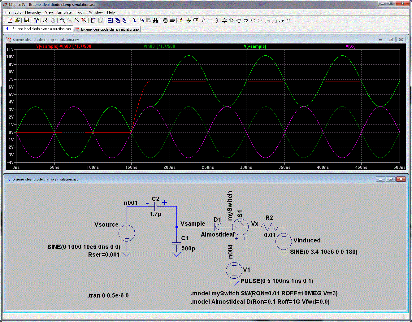
To illustrate this concept better, I've done some basic simulations using LTSpice. My simulation-circuit is a much simplified version of the part of Bruene's coupler that generates Vref. Please note that:
I've annotated the schematic below to describe the basic functions of each part of the simulation circuit.

So what's going on in the plots? Let's look...

I've defined an "Offset" voltage across C2. It can also be thought to be across C1, too, and it's effectively the amount that Vsample has been shifted. I'll explain this further a bit further down the post.
Looking at the plots, at 100nS we connect Vinduced to the diode and so at the 150 ns mark, when the voltage at Vsample is driven negative by Vsource, the diode's cathode connected to Vsample will start to go negative during the negative half-cycle of Vsource. Because the diode's anode is tied to a 0V source, the diode will turn ON when its cathode voltage drops about 0.7V below its anode voltage. I.e. when Vsample is approximately -0.7V.
When the diode turns ON, it effectively "clamps" the voltage at Vsample to -0.7 volts.
However, Vsource is still going negative. So we have the "+" terminal of C2 (see simulation schematic) clamped at -0.7V and C2's "-" terminal (attached to Vsource) continuing down, which causes charge to flow onto C2's plates. When Vsource reaches its negative peak, this charge can be calculated from the equation Q = C*V:
Actually, in the real world the voltage is slightly less than this by Vf, the forward voltage drop across the diode.
Now, as Vsource starts to rise again from its negative most transition, the diode turns off, but not immediately, which is the "real-world" diode turn-off effect you see on the Red line in the plot above.
With real-world diode effects, the plots can get a bit confusing, so let me introduce a simpler example that uses an "ideal" diode. I'll define the diode to have a Vf of 0V: if its Cathode is at all negative with respect to its Anode, it is ON, and if its Cathode is at all positive with respect to its Anode, it is OFF.
Shunt Rectifier with Vinduced as a DC source and an Ideal Diode:
Here's the circuit and the simulation:

Looks a bit cleaner, doesn't it?
So what is happening?
From 0-100ns the diode's Anode is floating because the switch is open, and it is essentially out of the circuit. Vsample is just Vsource divided down by the capacitive voltage divider (C1 and C2), and therefore Vsample goes between -3.4V and +3.4V. Its average value is 0V.
At 100ns the switch turns ON, and the diode's Anode is connected to Vinduced, which here is a 0VDC source.
From 100ns to 150ns, Vsource is positive and thus Vsample is still positive. The diode is OFF (it is back-biased: Cathode positive, Anode at 0VDC), and Vsample is still just Vsource divided down by the capacitive voltage divider (C1 and C2).
But starting at 150ns, Vsource goes negative and it tries to take Vsample below 0, too. But Vsample cannot go negative, because as soon as it begins to go below 0V, the diode turns ON and clamps it to the voltage at its Anode, 0VDC.
So as Vsource goes negative, Vsample sticks at 0V, and the voltage across C2 (1.7pf) gets larger and larger, until, at 175ns when Vsource is at its negative peak, the voltage across C2 (Vc2) is at its max:
At this point C2 will have its maximum charge on its plates. From the formula Q = C*V, we know that:
(...given the voltage at the diode's Anode is 0VDC and that the diode is ideal with a 0V Forward-voltage drop.)
Also, note that the voltage across C1 (500pf) is 0V (Vsample is clamped to 0V). Therefore the charge on C1 is 0 coulombs.
So at 175ns, when Vsource has reached its most negative excursion, the maximum charge is on the two caps:
Now, as time moves on from 175ns, Vsource just starts to rise up from its negative peak. Vsample, which was at 0 V, starts to go positive and the diode immediately cuts off (because Vsample = Vsource + Vc2(max)). The diode is now effectively out of the circuit.
The diode is back-biased and out of the circuit. There's no path for the charge of Qmax on C2 to go but to C1 (there's no other path but to C1). So, as time continues, no charge will by lost by the C1/C2 combo, and no charge will be added -- the diode never turns on again. And so the total charge on C2 and C1 (=Qmax) will flow back and forth between C2 and C1 as Vsource goes up and down.
No charge is being added, no charge subtracted. Therefore, at all times (after we've first charged C2 via the diode clamp), the charge across C1 and C2 must satisfy this equation:
And therefore (using Q = C*V):
Rearranging:
So, if we know Qmax (and we do), we can calculate what Vsample will be for any value of Vsource.
The equations above do this for an ideal diode with 0V attached to its anode. We can derive a more general equation for Qmax (rather than use equation 1 above) that takes into account the voltage connected to the diode's Anode and also its Forward-voltage drop (i.e. a non-ideal diode):
Using equations 2 and 3, we can now calculate Vsample for different voltages connected to the diode's Anode, per the table below (I'll keep the diode ideal, though, with Vf = 0):

You can see that "Vsample without diode" ranges from -3.4 to 3.4V. If we look at, say, the diode with 0V attached to its anode, the range of Vsample now becomes: 0V to 6.8V -- a shift of 3.4V, the peak voltage of the non-diode Vsample. So Vsample's average voltage is now 3.4 volts instead of 0, and if we were to filter out the AC waveform on Vsample we would measure 3.4 VDC.
The previous example was with a DC source connected to the diode's Anode and demonstrates how the shunt-rectifier can create a DC voltage from an AC signal. What happens if the Anode is instead connected to an AC source representing the voltage from the current-sample?
Vinduced as an AC source:
So all is fine and good if Vinduced is a DC source. Let's change Vinduced from a DC voltage source to something instead the simulates what is actually happening in the Bruene Coupler -- an AC source of the same frequency as Vsource, but with a phase offset.
We should still see a DC offset voltage generated on the capacitors in an analogous way to when Vinduced was a DC source. But the level of this offset voltage should now depend on the phase difference between the Vinduced and Vsource.
Let's examine how the voltage offset changes with phase (see the RED line in
the plots below). With the two waveforms 180 degrees out of phase,
LTSpice simulates this value to be 6.8V:
With the two waveforms 180 degrees in phase (0 degrees delta), LTSpice simulates this value to be 0V:

With the two waveforms 45 degrees out of phase, LTSpice simulates this value to be 2.61V:

With the two waveforms 180 degrees out of phase, LTSpice simulates this value to be 4.8V:

And finally, with the two waveforms 135 degrees out of phase, LTSpice simulates this value to be 6.28V:

Summarizing the DC offset calculated by the simulations:

But is this DC value that LTSpice calculates actually equal to the difference (or sum) of the two sine waves representing our voltage sample and current sample? This is a requirement that must be met if we are to calculate Vfwd and Vref by adding or subtracting the voltage and current samples.
Let's check this by doing some separate math, using the same peak voltages and phases that I used in the LTSpice examples above...
If summing sine waves, I can use the following equations to calculate the the resulting amplitude of the summed waveform (amplitude can be expressed as Vrms, Vpp, etc. I'll use Vpeak, which, from our simulations, is 3.4V).

Knowing the amplitudes of the sine waves and the different phases, I can plug these numbers into Excel and solve for c, the summed-amplitude (called Vc in the table, below):

The "LTSpice" column is 180 degrees out of phase with with "formula" column because the "shunt-diode" circuit is actually a differencer, not a summer, which is equivalent to adding 180 degrees to the phase shift "α" in the formula for c.
If we compare the table results from the math with our simulation results (see the earlier table), we find that they are exactly the same values (after first taking into account the shunt-diode's additional 180 degree phase shift). Which means that the shunt diode circuit is indeed summing (or differencing) the voltage waveforms of the voltage sample and the current sample!
And therefore, it is functionally equivalent to the earlier Bruene coupler variants that we looked at in Part 1.
Now that I've shown that the shunt-rectifier sums or differences the voltage and current samples, I'll refer you back to Part 1 for a recap of circuit operation in Transmission Line and non-Transmission Line environments.
The only thing to keep in mind is that, because the shunt-rectifier is actually a differencing circuit, not an adder, the side of the coupler that, in part 1, generated Vfwd (that is, the left side of the circuit in the diagrams), now generates Vref.
And the opposite side (the right side of the circuit in the diagrams) now generates Vfwd.
Other than that, the same analysis applies!
Bruene Variant, Daiwa SWR Meters:
While looking around the shack I came across a Daiwa CN-620B wattmeter that I pickup up several years ago. Opening it up, I discovered it's a variation of the Bruene Coupler that uses Bruene's "shunt rectifier" method of creating a DC voltage from the voltage and current samples.


The main differences that I can see between it and Bruene's design are:
Links to my Directional Coupler blog posts:
Notes on the Bruene Coupler, Part 2
Notes on the Bruene Coupler, Part 1
Notes on HF Directional Couplers (Tandem Match)
So, assuming you're familiar with the basic principles of the Bruene coupler, let's move on to Bruene's design!
Let's start with the schematic of the Bruene Coupler:
(click on image to enlarge)
This coupler was used in the Collins 302C-3 Directional Wattmeter and it was also described in an article written by Warren Bruene in QST magazine ("An Inside Picture of Directional Wattmeters," QST, April, 1959).
This architecture uses the same principles as the ones described in Part 1: to generate a voltage representative of a Forward Wave on a transmission line, a sample of the line current is added to a sample of the line voltage.
And to generate a voltage representative of a Reflected (or Reverse) wave on a transmission line, a sample of the line current is subtracted from a sample of the line voltage.
What differentiates Bruene's design from the other variations is that those variations keep the circuitry generating the voltage sample independent of the circuitry generating the current sample. Which is to say, with those other designs I could take a voltmeter and independently measure the voltage sample and the current sample. I cannot do that with Bruene's circuit -- voltage-sample and current-sample generation are bound together!
You're probably looking at the above schematic right now and wondering what the heck I'm talking about. You see two voltage dividers, so they must be generating the voltage sample of the Transmission Line voltage, while the transformer (with the two 10 ohms resistors) is generating a positive and negative voltage related to the current on the Transmission Line. Everything's copacetic, right?
But take a closer look.
Vfwd and Vref. which are the sum and differences of the voltage and current samples, are measured at the divider-taps of the two capacitive voltage dividers. So the voltage dividers can't just be generating samples of the Transmission Line's voltage. They must somehow be involved with summing in the Line current samples, too!
The key to the summing are the two diodes. But how are the diodes doing this?
Each diode is actually behaving as a "shunt rectifier" (see Chapter 2 in this >reference<). And this shunt-rectification process is differencing (rather than summing) the voltage-sample and the current sample that are at the diode's Cathode and Anode, respectively, with the result appearing at the diode's Cathode (the junction of the two voltage-dividing capacitors).
To illustrate this concept better, I've done some basic simulations using LTSpice. My simulation-circuit is a much simplified version of the part of Bruene's coupler that generates Vref. Please note that:
- I use the same capacitor values for the voltage divider as Bruene. Vsource is the voltage across the transmission line. It's a large amplitude because the voltage divider has a huge division ratio.
- The voltage created by the current-sampler, originally generated by a current source (the transformer) driving its current through the resistors, has been replaced by its Thevenin equivalent, but I've made the series-R very small to keep its effect from confusing this discussion. I've called this voltage source Vinduced.
- I've added a "switch" between the Diode's anode and Vinduced so that I can look at the voltage sample (at the voltage-divider tap) for a full 360 degree cycle without it being influenced by the current sample.
I've annotated the schematic below to describe the basic functions of each part of the simulation circuit.
(click on image to enlarge)
So what's going on in the plots? Let's look...
(click to enlarge)
I've defined an "Offset" voltage across C2. It can also be thought to be across C1, too, and it's effectively the amount that Vsample has been shifted. I'll explain this further a bit further down the post.
Looking at the plots, at 100nS we connect Vinduced to the diode and so at the 150 ns mark, when the voltage at Vsample is driven negative by Vsource, the diode's cathode connected to Vsample will start to go negative during the negative half-cycle of Vsource. Because the diode's anode is tied to a 0V source, the diode will turn ON when its cathode voltage drops about 0.7V below its anode voltage. I.e. when Vsample is approximately -0.7V.
When the diode turns ON, it effectively "clamps" the voltage at Vsample to -0.7 volts.
However, Vsource is still going negative. So we have the "+" terminal of C2 (see simulation schematic) clamped at -0.7V and C2's "-" terminal (attached to Vsource) continuing down, which causes charge to flow onto C2's plates. When Vsource reaches its negative peak, this charge can be calculated from the equation Q = C*V:
Q(max) = C2*Vsource(pk)
Actually, in the real world the voltage is slightly less than this by Vf, the forward voltage drop across the diode.
Now, as Vsource starts to rise again from its negative most transition, the diode turns off, but not immediately, which is the "real-world" diode turn-off effect you see on the Red line in the plot above.
With real-world diode effects, the plots can get a bit confusing, so let me introduce a simpler example that uses an "ideal" diode. I'll define the diode to have a Vf of 0V: if its Cathode is at all negative with respect to its Anode, it is ON, and if its Cathode is at all positive with respect to its Anode, it is OFF.
Shunt Rectifier with Vinduced as a DC source and an Ideal Diode:
Here's the circuit and the simulation:
(click on image to enlarge)
So what is happening?
From 0-100ns the diode's Anode is floating because the switch is open, and it is essentially out of the circuit. Vsample is just Vsource divided down by the capacitive voltage divider (C1 and C2), and therefore Vsample goes between -3.4V and +3.4V. Its average value is 0V.
At 100ns the switch turns ON, and the diode's Anode is connected to Vinduced, which here is a 0VDC source.
From 100ns to 150ns, Vsource is positive and thus Vsample is still positive. The diode is OFF (it is back-biased: Cathode positive, Anode at 0VDC), and Vsample is still just Vsource divided down by the capacitive voltage divider (C1 and C2).
But starting at 150ns, Vsource goes negative and it tries to take Vsample below 0, too. But Vsample cannot go negative, because as soon as it begins to go below 0V, the diode turns ON and clamps it to the voltage at its Anode, 0VDC.
So as Vsource goes negative, Vsample sticks at 0V, and the voltage across C2 (1.7pf) gets larger and larger, until, at 175ns when Vsource is at its negative peak, the voltage across C2 (Vc2) is at its max:
Vc2(max) = 1000 V.
At this point C2 will have its maximum charge on its plates. From the formula Q = C*V, we know that:
Qc2 @ max V = C2 * Vc2(max) = C2*Vsource(peak)
(...given the voltage at the diode's Anode is 0VDC and that the diode is ideal with a 0V Forward-voltage drop.)
Also, note that the voltage across C1 (500pf) is 0V (Vsample is clamped to 0V). Therefore the charge on C1 is 0 coulombs.
So at 175ns, when Vsource has reached its most negative excursion, the maximum charge is on the two caps:
Qmax = Qc1 + Qc2 = 0 + C2*Vsource(peak) (equation
1)
Now, as time moves on from 175ns, Vsource just starts to rise up from its negative peak. Vsample, which was at 0 V, starts to go positive and the diode immediately cuts off (because Vsample = Vsource + Vc2(max)). The diode is now effectively out of the circuit.
The diode is back-biased and out of the circuit. There's no path for the charge of Qmax on C2 to go but to C1 (there's no other path but to C1). So, as time continues, no charge will by lost by the C1/C2 combo, and no charge will be added -- the diode never turns on again. And so the total charge on C2 and C1 (=Qmax) will flow back and forth between C2 and C1 as Vsource goes up and down.
No charge is being added, no charge subtracted. Therefore, at all times (after we've first charged C2 via the diode clamp), the charge across C1 and C2 must satisfy this equation:
Qc1 + Qc2 = Qmax
And therefore (using Q = C*V):
C2*(Vsample - Vsource) + C1*Vsample = Qmax
Rearranging:
Vsample = Vsource*C2/(C1+C2) + Qmax/(C1+C2)
(equation 2)
So, if we know Qmax (and we do), we can calculate what Vsample will be for any value of Vsource.
The equations above do this for an ideal diode with 0V attached to its anode. We can derive a more general equation for Qmax (rather than use equation 1 above) that takes into account the voltage connected to the diode's Anode and also its Forward-voltage drop (i.e. a non-ideal diode):
Qmax = C2*(Vsource(pk) + V(anode) - Vf(diode)) + C1*(V(anode)
- Vf(diode)) (equation 3)
Using equations 2 and 3, we can now calculate Vsample for different voltages connected to the diode's Anode, per the table below (I'll keep the diode ideal, though, with Vf = 0):
(click on image to enlarge)
You can see that "Vsample without diode" ranges from -3.4 to 3.4V. If we look at, say, the diode with 0V attached to its anode, the range of Vsample now becomes: 0V to 6.8V -- a shift of 3.4V, the peak voltage of the non-diode Vsample. So Vsample's average voltage is now 3.4 volts instead of 0, and if we were to filter out the AC waveform on Vsample we would measure 3.4 VDC.
The previous example was with a DC source connected to the diode's Anode and demonstrates how the shunt-rectifier can create a DC voltage from an AC signal. What happens if the Anode is instead connected to an AC source representing the voltage from the current-sample?
Vinduced as an AC source:
So all is fine and good if Vinduced is a DC source. Let's change Vinduced from a DC voltage source to something instead the simulates what is actually happening in the Bruene Coupler -- an AC source of the same frequency as Vsource, but with a phase offset.
We should still see a DC offset voltage generated on the capacitors in an analogous way to when Vinduced was a DC source. But the level of this offset voltage should now depend on the phase difference between the Vinduced and Vsource.
To keep the analysis simple, I won't be changing the amplitudes of
Vsource or Vinduced, just their phase relationship. And
note that the amplitude of Vsource has been chosen so that, if the
diode were removed, Vsample = Vinduced in
amplitude.
(click on image to enlarge)
With the two waveforms 180 degrees in phase (0 degrees delta), LTSpice simulates this value to be 0V:
(click on image to enlarge)
With the two waveforms 45 degrees out of phase, LTSpice simulates this value to be 2.61V:
(click on image to enlarge)
With the two waveforms 180 degrees out of phase, LTSpice simulates this value to be 4.8V:
(click on image to enlarge)
And finally, with the two waveforms 135 degrees out of phase, LTSpice simulates this value to be 6.28V:
(click on image to enlarge)
Summarizing the DC offset calculated by the simulations:
But is this DC value that LTSpice calculates actually equal to the difference (or sum) of the two sine waves representing our voltage sample and current sample? This is a requirement that must be met if we are to calculate Vfwd and Vref by adding or subtracting the voltage and current samples.
Let's check this by doing some separate math, using the same peak voltages and phases that I used in the LTSpice examples above...
If summing sine waves, I can use the following equations to calculate the the resulting amplitude of the summed waveform (amplitude can be expressed as Vrms, Vpp, etc. I'll use Vpeak, which, from our simulations, is 3.4V).
Knowing the amplitudes of the sine waves and the different phases, I can plug these numbers into Excel and solve for c, the summed-amplitude (called Vc in the table, below):
(click on image to enlarge)
The "LTSpice" column is 180 degrees out of phase with with "formula" column because the "shunt-diode" circuit is actually a differencer, not a summer, which is equivalent to adding 180 degrees to the phase shift "α" in the formula for c.
If we compare the table results from the math with our simulation results (see the earlier table), we find that they are exactly the same values (after first taking into account the shunt-diode's additional 180 degree phase shift). Which means that the shunt diode circuit is indeed summing (or differencing) the voltage waveforms of the voltage sample and the current sample!
And therefore, it is functionally equivalent to the earlier Bruene coupler variants that we looked at in Part 1.
Now that I've shown that the shunt-rectifier sums or differences the voltage and current samples, I'll refer you back to Part 1 for a recap of circuit operation in Transmission Line and non-Transmission Line environments.
The only thing to keep in mind is that, because the shunt-rectifier is actually a differencing circuit, not an adder, the side of the coupler that, in part 1, generated Vfwd (that is, the left side of the circuit in the diagrams), now generates Vref.
And the opposite side (the right side of the circuit in the diagrams) now generates Vfwd.
Other than that, the same analysis applies!
Bruene Variant, Daiwa SWR Meters:
While looking around the shack I came across a Daiwa CN-620B wattmeter that I pickup up several years ago. Opening it up, I discovered it's a variation of the Bruene Coupler that uses Bruene's "shunt rectifier" method of creating a DC voltage from the voltage and current samples.
(click on image to enlarge)
Inside the Daiwa CN-620B (click on image to enlarge))
The main differences that I can see between it and Bruene's design are:
- Daiwa uses two transformers, one for Vref for Vfwd, compared to Bruene's one.
- The Daiwa transformers have fewer windings than Bruene's (I believe the latter has 60).
Links to my Directional Coupler blog posts:
Notes on the Bruene Coupler, Part 2
Notes on the Bruene Coupler, Part 1
Notes on HF Directional Couplers (Tandem Match)
Building an HF Directional Coupler
Notes on the Bird Wattmeter
Notes on the Monimatch
Notes on the Twin-lead "Twin-Lamp" SWR Indicator
Calculating Flux Density in Tandem-Match Transformers
And some related links from my Auto-Tuner and my HF PA posts:
Auto Tuner, Part 5: Directional Coupler Design
Auto Tuner, Part 6: Notes on Match Detection
Auto Tuner, Part 8: The Build, Phase 2 (Integration of Match Detection)
HF PA, Part 5: T/R Switching and Output Directional Coupler
Bruene Coupler References:
Bruene, Warren, "An Inside Picture of Directional Wattmeters," QST, Apr., 1959. Includes both a good explanation of the Monimatch operation and a design for a directional wattmeter whose directional coupler topology would later be known as the "Bruene Coupler."
Collins 302C-3 Directional Wattmeter, PDF Manual containing schematic.
Rush, James, Jr., "The Mini-Mono-Monimatch," QST, Mar., 1965. Although called a Monimatch in the title, the design is actually more similar to Bruene's directional coupler.
Bold, Gary, ZL1AN, "The Bruene Directional Coupler and Transmission Lines," PDF. This PDF gives an excellent explanation of the Bruene Coupler.
Kiciak, Paul, N2PK, "An HF In-Line Return Loss and Power Meter," PDF. Constructions details of a power meter using a Bruene Coupler. Contains an explanation by the other of why he prefers the Bruene coupler of the Tandem-Match Coupler. Also interesting because the author separates the voltage-sampler from the current sampler and uses the differential inputs of an AD8307 to do the required addition (or subtraction) to get FWD and REF voltages.
(This web page could be useful for understanding the sampling method used in the N2PK meter: http://www.g3ynh.info/zdocs/bridges/magdiff/part1.html )
Lewallen, Roy, W7EL, "A Simple and Accurate QRP Directional Wattmeter," QST, Feb, 1990, PDF. Interesting variant of the Bruene coupler. Roy uses two transformers for the voltage sample in lieu of capacitor voltage dividers.
White, Ian, G3SEK, "Inside a Directional Wattmeter," RadCom, Sept., 2002, PDF. Discussion and a bit of analysis of Bruene coupler. Includes Bruene's phase-relationship diagrams.
http://www.g3ynh.info/zdocs/bridges/reflectom/part1.html interesting analysis
http://www.g3ynh.info/circuits/Diode_det.pdf Diode detectors -- includes some info on shunt detectors, which is what Bruene's design uses.
Other references of generally interest:
http://www.g3ynh.info/zdocs/bridges/Xformers/part_1.html great discussion on current-transformers for directional coupler applications
http://www.g3ynh.info/zdocs/bridges/Xformers/part_2.html Part 2 of current-transformers
http://www.g3ynh.info/zdocs/bridges/Xformers/part_3.html And part 3, the last part, of current-transformers
http://www.g3ynh.info/zdocs/bridges/index.html Indexes numerous topics. Lots of great info to be found here!
http://www.richtek.com/assets/AppNote/AN008_EN/AN008_EN.jsp Common-Mode choke model
Final Caveats:
As always, I might have made a mistake in my equations, assumptions, or interpretations. If you see anything you believe to be in error, or if anything is confusing, please feel free to contact me.


1 comment:
Thanks for your great analysis and knowledge sharing, especially the role of shunt diode playing in the Bruene coupler. In addition to the analysis, i am interesting in more realisitc things, what starys and parasitics we should pay more attention to when we are trying to select the diode, or the voltage divider...etc. So it'd be much appreciated if you can send me some notes about these stuff.
Thank,
Walter
Post a Comment