Wednesday, August 16, 2017

An FPGA SDR HF Transceiver, Part 8 -- Front Panel, Rear Panel, and Other Schematics

In this eighth blog post in my FPGA SDR Transceiver series, I will describe the Front Panel and its Arduino processor (and associated circuitry), the Rear Panel, and other circuitry within the radio that interconnects front panel with rear panel.

(Part 7 of this series is here: Part 7)


Before I begin, let me again acknowledge Dick Benson, W1QG.  Dick is the father of this design, and although I've made some modifications to the FPGA logic, the underlying architecture and the vast majority of the Simulink implementation is Dick's.


A note regarding the schematics...

These schematics were drawn using the Lite version of Cadence's Orcad Capture.  This is the free version of the program, and it limits a schematic's number of nets to 75 and the number of parts to 60 (limitations which apply if you want to save the design, which I always do).

Because this radio design has many more nets and parts than the 75/60 limit specified by Cadence, I have broken the overall design into smaller "bite size" schematics, each  independent of the others and each drawn on a single A-size sheet.

But because I've broken up the design into smaller independent pieces, I can not use Capture's Design Rule Checker to check the overall design for design flaws.  Therefore, there is the possibility that errors have crept into the schematics.  So be aware!


Summary:

The Front Panel provides the User Interface for the radio, and it is designed to be a separate sub-assembly that can easily be removed from the chassis.

An Arduino Nano processor provides the user-interface processing, and it is tasked with reading the front and rear panel controls, displaying information on the LCD, and communicating with the FPGA.

Let's take a look at the schematics...


Front Panel Main (Nano) Board Schematics:

(Click on image to enlarge)

Notes on the "Main" board schematic:
  1. +12V is supplied to the board via J11 in the lower right-hand corner.  This +12V will also power the FPGA board (via header J1).
  2. +5V is also supplied to the board from a separate source (via J12) -- the Arduino Nano's on-board 5V regulator cannot supply the current required at 5V for the front panel, and so a separate switching power supply provides this assembly's 5V power.
  3. J1 is the primary interface to the FPGA board, and it supports the 4-wire Control Interface, provides +12V to the FPGA board, and carries other miscellaneous IO signals (such as mic audio) between the FPGA board and the Front Panel.
  4. Note that the FPGA Control Interface is a 3.3V interface, whereas the Arduino's IOs are 5V.  R9 and R10 (in conjunction with terminating resistors on the FPGA board) divide down the 5V control signals sent from the Arduino to be 3.3V compliant for the FPGA, and U2 and U3 provide a level translation of FPGA 3.3V output signals to input levels compatible with the Arduino's 5V IO. (Note that the Arduino's ViH spec is 3.0V, minimum, which is slightly higher than the Xilinx FPGA minimum VoH spec of 2.9V.  Thus the level translators to ensure that the Xilinx outputs meet the Arduino's ViH spec.) 
  5. U4 provides 3.3 volts for the Main board.
  6. The front panel's Volume control provides a voltage that is converted to digital by the Arduino (and then sent to the FPGA via the 4-wire Command Interface).
  7. Transmit SWR and Forward Power can also be sampled by the Arduino's ADC via connector J6.  (At this time this feature is not used for monitoring power and SWR.  Instead, these pins are used to measure the input DC Voltage (e.g. 13.5 VDC).  This feature is described further, below, in the Interconnects 1 notes).
  8. The board also has a buzzer, LS1, to provide various beeps when I press buttons or when error conditions occur.  The Arduino pin driving this beeper can also be used to "calibrate" the Arduino's ADC readings  (to compensate for the actual ADC reference voltage -- necessary if trying to use VRL and VF to calculate SWR and Forward Power).  Its function is selected via header J10.
  9. There are simple one-pole RC filters on many of the IO signals to mitigate susceptibility to RF fields that might be coupled onto external cabling and leads.
  10. LED D2 is an on-board LED used only for debugging and is not visible during normal radio operation (its function is duplicated by a second LED, to be described later, below).

(Click on image to enlarge)

Notes on the "IO1" Schematic:
  1. This schematic shows two headers that provide IO signals to the Arduino.
  2. The upper header, J21, connects to the rotary encoder used for frequency tuning (this is an Oak/Grigby Rotary Optical Encoder, Model 91Q128-43-00110, that provides 128 pulses per revolution).
  3. The lower header, J22, connects to the two front-panel mechanical rotary encoders and the analog meter.  These rotary encoders include push-button switches and are used to select menu items via the LCD.  (They are similar to those used in the Keyes KY-040 rotary encoder module).
  4. Again, simple one-pole RC filters attenuate any RF that might be coupled into the circuitry via external wiring.

(Click on image to enlarge)

Notes on the "IO2" Schematic:
  1. There are more IO signals than there are Arduino IO pins: U1 is an IO expander (PCF8575) that allows the Nano access to the additional IO signals.  It communicates with the Arduino Nano via the Nano's I2C interface.
  2. The RST signal from U1 is a high-true Reset signal, sent to the FPGA board, used for resetting the FPGA's Communications Interface.  Note that the PCF8575 cannot drive its output pins high, so a pullup is needed (R23).
  3. The Arduino also communicates with the LCD via I2C (using an external I2C to parallel converter mounted at the LCD).  Header J2 provides this interface.
  4. Header J16 provides an extra I2C connector.  It is not used at this time.
  5. The microphone audio attaches to the Arduino board via header J13.  Note that the microphone audio is not used by the Arduino -- instead, this signal is simply routed to the 26-pin FPGA interface connector, where it is sent to the FPGA board (and converted into a digital signal).  By the way, this MIC_AUD signal is not from the mic connector itself, but from a separate mic preamp board that will be described later, below).
  6. U4 provides "clean" 5V that can be used to power an active (FET) mic element.  This feature is not used at this time.
  7. Transmitter keying is controlled via the Arduino, and the signal nPTT (low true) is used both in CW and Voice modes to signal the FPGA (via the Arduino) to Transmit.  Because this signal can come from the outside world, I've added ESD protection with TVS1.  (R8 provides both RF filtering and current-limiting if TVS1 were to clamp).
  8. And again, numerous simple RC filters on control lines to filter out RF that might be coupled onto cabling.
  9. The LED is only used for debugging and is not visible during normal operation of the radio.

Connector Locations:

For my own records, below are the location of the Main Board's connectors (shown in the three schematics, above):


Front Panel 5V Switcher:

The Front Panel's 5V requirements are supplied by a 5V switcher that converts 12V to 5 VDC.  (I had originally used an LM7805 linear regulator, but, given the 5V rail's load current, the 7805 was getting too hot for comfort even with a large heat-sink, and so I went the switcher route.

This circuit is mounted on a separate board within the Front Panel assembly (it is not on the Arduino "Main" board).

(Click on image to enlarge)

The circuit should be self explanatory.  For additional information refer to the LM2576 datasheet.


Front Panel Controls:

Now let's look at the wiring of most of the front panel's controls.  (The remaining controls will be described in the next section, below).

This circuitry should be self-explanatory...

(Click on image to enlarge)

(Click on image to enlarge) 


Front Panel Controls, Rear Panel, and Interconnects:

Below are the remaining front panel controls and connectors, as well as rear panel connectors and how they all interconnect.

(Click on image to enlarge)

Notes on the "Interconnections 1" schematic:
  1. On the rear panel, diode D1 provides protection against accidental reversing of the power supply voltage.
  2. J15, the "EXT. ON" connector, provides a signal for external devices that is low-true when the FPGA SDR radio is ON. 
  3. J3 provides a PTT port parallel with the front-panel's "Key" and "MIC" (PTT pin) ports.  Note that this signal, nPTT, is low true (low = xmit).
  4. The input DC voltage can be monitored (and thus displayed on the LCD) by the Arduino.  This DC voltage is sampled after the Schottky diode on the rear panel and then divided-by-four.  The resulting voltage, on Header J37, is connected to J6 on the Arduino board via a 3-wire cable.  Either J6 pin 1 or J6 pin 3 can be read by the Arduino's ADC, the ADC reading then multiplied by 4 (and with an offset representing the Schottky Diode D1's Vf drop added to this result) to represent the voltage at J34.

This next schematic, "Interconnects 2", details the audio output interconnections:

(Click on image to enlarge)

Notes on the "Interconnects 2" schematic:
  1. Speaker Audio from the FPGA board comes into this schematic via connector J12 (at bottom of schematic).
  2. LS1 is the radio's internal speaker (mounted on the top cover).
  3. An external speaker can be connected to the radio via J1 on the back panel.  Plugging in an external speaker will turn OFF the radio's internal speaker.  (Important note: the external speaker should be connected only to Tip and Ring of the stereo plug, NOT to ground).
  4. Although a stereo connector (J2) is used for the headphones, they are connected in MONO mode (left and right in parallel).
  5. And because the speaker audio from the FPGA board is differential with DC bias, this differential signal is converted to single-ended for the headphones by using just one side of the differential signal (against ground).  The DC bias is removed by C1 (i.e. the audio is AC-coupled to the headphone jack).
  6. R3 keeps the negative side of C1 at ground potential so that there isn't a loud "pop" in the headphones when they are plugged into J2.
  7. The SPKR ON switch turns ON or OFF any speaker (internal or extenal), but not headphone audio.  One side of this switch is read by the Arduino, and the switch status is sent to the FPGA where it is used to change the audio level when headphones are used.

Below is an image showing the interconnects in the two schematics above.

(Click on image to enlarge)

(Note some singeing on the wires going to J12.  Oops!  Also, J37 was originally a 4 pin header.  It has been trimmed down to 3 pins.)


The next schematic details the small "plate" (actually double-sided PCB stock) upon which two RJ45 connectors are mounted:

(Click on image to enlarge)

Notes on the "RJ-45 Plate" schematic:
  1. The two headers on the left-hand side connect to the main FPGA board (described in post 6 of this blog series).  The "Interconnects 3" and the "Interconnects 4" schematics can be found there.
  2. I plan to use an SDR1000 PA (plus a driver board) to amplify the FPGA SDR Radio's TX output up to 100 watts, peak power.  This PA and driver will be mounted in an external chassis and controlled by the FPGA SDR via connector J1 in the schematic (above), which will connect to the separate PA assembly via a shielded RJ-45 cable.
  3. I also have plans to build an external 500 watt solid-state PA.  Similarly, it will connect to J5 in the schematic (above) via a shielded RJ-45 cable.
  4. To prevent EMI coupled onto external wiring from getting into the radio, all IO from the RJ45 pass through simple one-pole RC filters.  These should be placed as close to the RJ45 connectors as possible.


*** Schematics of additional rear-panel connectors will go here.


I'm using a scrap HP 37203A HP-IB Extender as the chassis for this radio.  The original back panel looked like this:


Currently, it now looks like this:


(Note that I am adding connectors as I need them, so not all connector locations are populated yet).


LCD Adapter:

To minimize Arduino IO pin usage, the Arduino communicates with the Front Panel LCD via its 2-wire I2C interface.

But because the LCD itself does not support I2C, I use an I2C Interface LCD Adapter similar to the one shown below and available via eBay:


This adapter is designed for use with LCD modules having a 16-pin SIP interface connector.  Unfortunately, the LCD module I chose has a 16-pin DIP interface connector.  So I wired an adapter board (that sits on the back of the LCD module) to convert the I2C Adapter's 16-pin SIP wiring to 16-pin DIP wiring:

(Click on image to enlarge)

Microphone Preamp:

Microphones typically generate low-level audio.  Although the FPGA could internally amplify a low level signal coming into it via the 16-bit audio ADC (the AK4554 Codec), this amplification (following the ADC) also increases the noise-floor underlying the microphone audio.

So I've added an external Mic Preamp (prior to the audio codec) with three levels of gain:  26 dB, 16 dB, and 6 dB.  Its circuit is below:

(Click on image to enlarge)

Notes on the Microphone Preamp:
  1. An on-board 5V regulator (U2) provides "clean" power for the preamp circuitry. 
  2. The op-amp (U1) has rail-to-rail outputs.
  3. One half of the op-amp (U1A) is not used.  I prefer not to have floating inputs on ICs, so I've connected it in a non-inverting configuration with its output set to 2.5V.
  4. The MIC IN connector (J2) connect to the front panel microphone jack.
  5. The MIC OUT connector (J1) connects to the Arduino board, which passes the amplified microphone audio to the FPGA board and the audio codec there.
  6. TVS1 provides ESD protection against an ESD event occurring on the external MIC signal.
  7. The circuit originally started out with gains of 0, 10, and 20 dB.  I increased these by 6 dB by paralleling the original R8 (20K ohms) with another 20K (because it's easier to piggyback surface mount components than to remove and replace them), and then changing the input series capacitance from 200 nF (two 100 nF caps in parallel) to 400 nF (four 100 nF caps in parallel), to keep the high-pass cutoff at 40 Hz.

Assembly:

The HP case I'm using for the radio is not large, and so to install the Front Panel and its circuitry some creative assembly was required.  The photos below show what is involved...

First, here is the Front Panel with controls, LCD, encoders, and LCD Adapter and 5V switcher mounted (the 5V switcher is mounted (on standoffs) above the Frequency rotary encoder and the LCD Adapter is mounted (on standoffs) above the LCD module):


Next, mounting (on more standoffs) the Main (Arduino) board and the Mic Preamp board above the LCD Module Adapter and 5V switcher boards:


And finally, connecting all of the cables!

(Oh what a tangled web we weave!)


OK.  That's it for this blog post!


Background Notes:

SDR Notes:  Weaver Modulation and Demodulation
SDR Notes:  The Mixer Mathematics of Digital Down Conversion


Posts in this Series:

Part 1: Overview
Part 2: FPGA Modulation and Demodulation
Part 3: Interpolation and Decimation Filters
Part 5: Control Interface, Etc.
Part 9: 50 dB HF RF Power Amplifier


Standard Caveat:

I or Dick might have made a mistake in our designs, equations, schematics, models, etc.  If anything looks confusing or wrong to you, please feel free to comment below or send me an email.

Also, I will note:

This design and any associated information is distributed in the hope that it will be useful, but WITHOUT ANY WARRANTY; without even the implied warranty of MERCHANTABILITY or FITNESS FOR A PARTICULAR PURPOSE.

Thursday, July 13, 2017

An FPGA SDR HF Transceiver, Part 7 -- Schematics, RX and TX Signal Chains

In this seventh blog post in my FPGA SDR Transceiver series, I will describe the Receiver input circuitry -- the Receiver's Signal Chain, prior to the ADC:
  • RX Attenuator
  • Broadcast-Band Filter.
  • Anti-Aliasing Filter
  • Preamp and ADC Driver
Also, I will describe the Transmitter's output circuitry contained within the primary radio chassis -- that is, the Transmitter's Signal Chain.

(Part 6 of this series is here: Part 6)

But first, a teaser photo...


...which shows the radio as it is slowly being assembled into an old HP chassis I've scavenged for this purpose.

And before I begin, let me again acknowledge Dick Benson, W1QG.  Dick is the father of this design, and although I've made some modifications to the FPGA logic, the underlying architecture and the vast majority of the Simulink implementation is Dick's.


A note regarding the schematics...

These schematics were drawn using the Lite version of Cadence's Orcad Capture.  This is the free version of the program, and it limits a schematic's number of nets to 75 and the number of parts to 60 (limitations which apply if you want to save the design, which I always do).

Because this radio design has many more nets and parts than the 75/60 limit specified by Cadence, I have broken the overall design into smaller "bite size" schematics, each  independent of the others and each drawn on a single A-size sheet.

But because I've broken up the design into smaller independent pieces, I can not use Capture's Design Rule Checker to check the overall design for design flaws.  Therefore, there is the possibility that errors have crept into the schematics.  So be aware!


Block Diagram:

(Click on image to enlarge)

Notes on the block diagram:
  • The Receive Signal Chain begins at the T/R relay, shown above in Receive mode.
  • The first block is a variable attenuator, which can select 4 values of attenuation in 6 dB increments.
  • Next is filtering.  Broadcast-band stations in my area can be quite loud, so there is a high-pass filter to attenuate the broadcast band.  
  • And to prevent frequencies greater than half the ADC's sampling rate (that is, 80 MHz / 2, or 40 MHz) from being aliased down to the 0 - 40 MHz range, there is a low-pass anti-aliasing filter.
  • And finally, there are two stages of pre-amplification, which provide a total of 32 dB of gain prior to the ADC.
  • The Transmit Signal Chain consists simply of a low-pass Reconstruction Filter.

Note that there is no band-pass filtering prior to the ADC.  That is, as shown above, the receiver's front-end is wide open between 3 and 30 MHz.  So it is very important that the active preamplification stages be low-distortion.

Will additional front-end band-pass filtering be required?  So far the receiver seems to perform well running with its "wide open" front end (and broadcast-band filter).  But I'll give it some time to see if additional filtering is needed, and I will update this blog if I discover that some sort of front-end band-pass filtering improves performance.

RX-Chain, Attenuator and T/R Switch:

(Click on image to enlarge)

Notes on the RX Attenuator and T/R Switch.
  • The first relay (LS3, in the upper left corner) is simply a "receiver protection relay" that shorts the antenna input (and disconnects the radio circuitry from the antenna) when power is OFF.  (In the summer there are often thunderstorms in the Sierra Nevadas, and I'd like to protect the circuitry when I am not using the radio.
  • Relay LS4 is the T/R relay.  Note that the receiver input is grounded when in TX mode, and the transmitter output is connected to a 50 ohm load when in RX mode.  The relay contacts are connected in parallel, to reduce the possibility of flakey contacts causing problems.
  • The attenuators are nothing special -- standard PI configurations that can be switched in or out.  But note that relay LS2 is a 5V relay (all the others are 12V).  I ran out of 12V relays while building this circuit and so I instead used a 5V relay from my junkbox.  R15 limits its current to about 20 mA (when the DC input voltage is 12V).
  • After the attenuators there is a bit more receiver circuit protection consisting of a fuse and a TVS surge-protection device.  The TVS device should shunt to ground large voltages that exceed its threshold.  In doing so, if the current it is sinking is large (i.e. this is a serious over-voltage event!), the series fuse (63 mA PicoFuse) should blow.  Hopefully both of these devices will protect the receiver front-end circuitry.  (I haven't tested them to verify).
  • The fuse is paralleled with a header to allow me to easily check with an ohmmeter if the fuse has been blown (or short it out, if it has).
  • Diodes are placed across relay coils as standard practice to clamp voltage spikes on a collector of a relay drive transistor (e.g. Q1, Q2, or Q3) when a relay is turned off.  Caps were added across the diodes to shunt any RF (e.g. from nearby transmitters) that might get on the relay control lines.  Probably not needed, but there is no harm in having them.  By the way, the rule of thumb regarding diodes-across-relays is that their forward-current rating should be greater than the relay's "ON" current.  In the case of the relays I am using, their ON current is about 10 mA (at 12 V -- it will be a bit higher if DC power were, say, 13.5V).  (Note, I have not verified if the "rule of thumb" I just mentioned is indeed valid!).
  • Control signals from the FPGA board are filtered with simple one-pole low-pass R-C filters at point-of-entry to this circuit in an attempt to minimize (hopefully) any noise on these lines from being coupled to the sensitive RF front-end circuitry. 

By the way, there are any number of ways to implement an attenuator.  I had originally planned to use a Mini-Circuits DAT-31A-SP Digital Step Attenuator, and had thus planned that the Control I/F for the attenuator, from the FPGA, to consist of 3 bits (Serial Data, Serial Clock, and Latch Enable), in addition to +12V power and the T/R relay control line.  (I changed my mind before implementing this and went the relay route, simply because I did not want to solder the QFN-style package).

Dick (W1QG), on the other hand, rolled his own pin-diode attenuator design, using a UM4000 high-power PIN diode and with the amount of attenuation controlled via a front-panel control (potentiometer).  Regarding his design, here are Dick's words...

The IMD introduced by the PIN diode gain control was quantified.    

The experiment was as follows ....

1) Two  HP 3335A generators were summed.   F1=3.5 MHz  F2=4.0MHz.
2) Summed outputs fed to a variable attenuator which attenuates the summed signal so that the resulting signal, at the ADC, is 1 dB below where the ADC Overload led comes on.
3) Radio tuned to 3.5 and 4 MHz shows 36dB over S9 (that is FS for my rig), full gain (no PIN attenuation)
4) Radio then tuned to 4.5 MHz and signal is S2.  (S2 to S9 is 7*6=42 dB and then add 36 to get 78 dB which would be 84dB  below PEP.)
5) Add in PIN attenuation and the IMD3 term goes no where but DOWN, and quickly disappears. 
6) Radio was then tuned to 7.5 MHz to pick up the IMD2 product which was also S2.
7) The PIN attenuation was then increased as before.
This time the IMD2 did increase to just a bit over S3, but then quickly went down with further PIN attenuation. 
Perfect? No. But more than good enough for me especially since my RF gain control is parked at full tilt 99% of the time. 
Frankly, in retrospect, I probably should not have wasted the panel space for that control J

(Dick added a later note, below).

I had an idea at 0400 this AM regarding the small increase in IMD2 with the onset of the PIN attenuator. 

It precipitated a change (adding a second PIN diode) and this worked as I had hoped:  there is now ZERO increase in IMD2. 

At this point I would call the PIN attenuator PERFECT.  

Here is a schematic of Dick's PIN-Diode Attenuator:

(Click on image to enlarge)

Notes on the W1QG PIN-Diode Attenuator:
  1. The two diodes are in series, therefore the same amount of DC current flows through each.
  2. Capacitor C5, a 27 nF feedthrough cap, serves two purposes:  it filters noise, and it is an RF ground for the Anode of D1.

RX-Chain, Broadcast-Band and Anti-Aliasing Filters:

(Click on image to enlarge)

Notes on the Broadcast-Band (BCB) and Anti-Aliasing (AA) Filters:
  • The BCB Filter is a W1QG design.  160 meters is sacrificed to keep the filter simple, otherwise it would need to be more complex if we needed a good 1.8 MHz response while rejecting frequencies of 1.7 MHz and below.
  • Note that if some BCB feedthrough is desired (if you like listening to AM), Dick mentions that replacing the trace to ground (labeled 'A' in the schematic, above) with 16.6 nF of capacitance provides a good compromise between rejecting and passing AM stations.
  • The anti-aliasing filter is a Mini-Circuits "RLP-30+" surface-mount Low Pass Filter.  I chose it (rather than rolling my own) because of the ease of using it -- I found a seller on eBay who sells PCB boards for mounting them (search eBay for "mini-circuits GP1212 board".  By the way, it isn't that hard to cut your own pattern in copper-clad PCB stock if you'd rather make your own board).
Regarding the Anti-Aliasing Filter specifically:
The goal of the Anti-Aliasing Filter is to reject frequencies above 40 MHz (i.e. above the Nyquist frequency).  The RLP-30+ specified -3dB point is actually at 37 MHz, so there will not be too much attenuation of frequencies at 40 MHz or close to 40 MHz (e.g. 45 MHz).

Here is its frequency response:

(Click on image to enlarge)

Will this be a problem for me?  I only plan to use this radio to 30 MHz.  For a higher frequency to be "aliased" down to 30 MHz, that frequency would need to be 50 MHz (given the 80 MHz ADC sample rate).  And at 50 MHz, the RLP30+ provides at least 40 dB of attenuation (per my measurements, shown later in this post).

So far this amount of attenuation (and the slope of attenation between 40 and 50 MHz) has proven adequate.  If, with more usage, I find there to be a problem (for example, if there is a nearby high-power 6-meter or FM broadcast station), I can either add some additional filtering to the RLP-30+, or I can replace it with a more complex L-C filter.


RX-Chain, Preamp and ADC Driver:

The receiver's front-end gain-stage consists of a Preamp and ADC driver providing roughly 34 dB of gain to the ADC input (max ADC input is +7 dBm for ADC full-scale).

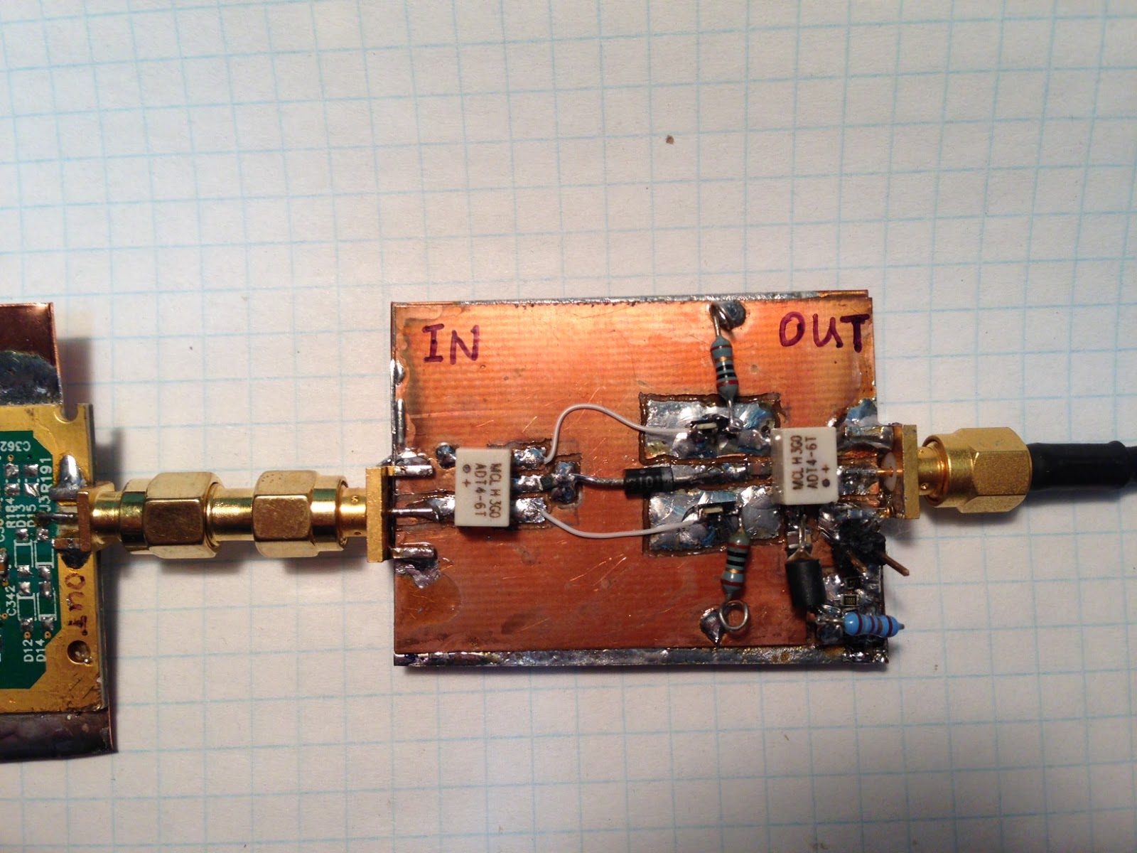
The Preamp consists of two Mini-Circuit's GALI-74 preamps connected in a push-pull configuration (to minimize second-order distortion, compared to a single-ended preamp).  Its gain is about +24 dB:

(Click on image to enlarge)

This stage was actually scavenged from a scrapped TCI board.  Using tin-snips, I cut out the push-pull GALI-74 section of the board from the TCI PCB, removed unnecessary parts, and added SMA connectors and a two-pin header for power:


Notes on the GALI-74 Preamplifier:
  • The preamplifier is push-pull to minimize even-order distortion.
  • Each GALI-74 is biased at 80 mA (for 160 mA, total).
Dick's second gain stage, the ADC Driver, is shown below.  It provides an additional 10 dB of gain:

(Click on image to enlarge)

Notes on the ADC Driver.
  • Again, this stage is push-pull to minimize even-order distortion.
  • Each transistor is biased at about 50 mA of collector current (100 mA, total).
Here's my implementation of this circuit:


To keep the radio's design simple, there is minimal front-end filtering (just an anti-aliasing filter and a broadcast-band reject filter).  So it is very important that the receiver's front end have good IM2 and IM3 performance (the reason why is explained in a bit more detail later in this post, when Dick describes his LTC6433 testing).

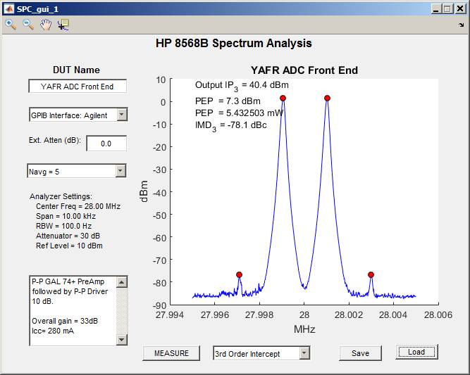
Here are my measurements (using my 8568B) of IM3 and IM2 performance of the GALI-74 preamp cascaded with the push-pull ADC driver.  Note that the levels are set so that the PEP output of the cascaded stages is about +7 dBm, which is the level required to drive the ADC input to full-scale:

IM3:


IM2:


For comparison, here are Dick's measurements (measured with his own 8568B) of the IM3 and IM2 performance3 of his GALI-74 preamp cascaded with the push-pull ADC Driver:


Per Dick:  IMD2 is now about 84dB down from PEP and I am pleased with that result.    

For completeness, Dick also ran a Noise Figure measurement on his GALI-74 preamp cascaded with the push-pull ADC Driver:


One more note:  the GALI-74 Preamplifier and the ADC Driver are both powered at +9VDC, which I create with an LM7809 voltage regulator.  I haven't included this regulator in my schematics.    For more information on this design, please refer to the LM78xx series of regulators datasheet for their recommended circuit.


RX-Chain, Overall Gain and Bandwidth:

Below are my measurements of the Rx-Chain's overall Gain and Bandwidth between the radio's Antenna Port and the Output Port of the Push-Pull ADC Driver stage.

In other words, the overall gain and bandwidth of the circuit blocks circled in orange, below.

(Click on image to enlarge)

To make this measurement, after S21 (i.e. "Response") calibration I added an additional 30 dB of attenuation between my Network Analyzer's output port and the FPGA SDR's antenna port.  Therefore, the horizontal "red" line in the image below represents + 30 dBm.

(Click on images to enlarge)

Notes on this response:
  • Frequency range is 1 MHz to 100 MHz.
  • Internal RX Attenuator set to 0 dB of attenuation.
  • Overall again in the passband is about +33 dB (given that the horizontal red line represents +30 dB of gain).
  • By 50 MHz the gain has dropped by more than 40 dB.
  • The PicoFuse I added for front-end protection adds roughly 0.5 dB of loss (per measurements.  Note that is has about 6 ohms of resistance, measured at DC).

The image below shows the left side of the above response zoomed in.


Notes:
  • The horizontal red-line on the 8753C Network Analyzer represents +30 dBm.
  • At 1.8 MHz, the response is 30 dB down from the passband.
  • There is a slight amount of passband droop at the start of the passband, but it is only about 1 dB and in my opinion not significant.  

And here's that same zoomed-in response, but with 18 dB of "internal" receive attenuation added.


Looks good!  18 dB of attenuation, as expected.


TX Chain:

The TX Chain consists solely of a Reconstruction Filter following the DAC.  I'm using the same Mini-Circuits RLP-30+ Low-Pass Filter that I used as the RX Chain's Anti-Aliasing Filter.

Here is the schematic:

(Click on image to enlarge)

Notes on the "TX Chain Reconstruction Filter":
  1. The highest transmit frequency that I'll be using is 29.7 MHz, which will result in an image at 50.3 MHz (given a Nyquist Frequency of 40 MHz).
  2. At 50.3 MHz the Reconstruction Filter's attenuation is at least 40 dB (measured).  This attenuation, coupled with the external PA's low-pass output filtering, should keep any images above Nyquist well down in amplitude.
  3. Output of the TX Chain (to the Antenna) is roughly 0 dBm, peak.
By the way, the DAC itself will have a sin(x)/x roll-off, characterized by this equation:

H(f) = sin(πf/fs)/(πf/fs), where fs is the sampling frequency (80 MHz in this design).

So the DAC output decreases with increasing frequency.  For example, the peak DAC output at 29.7 MHz will be about 2.04 dB lower than the peak DAC output at 3.5 MHz.


Other Design Notes:  LTC6433 Testing:

Before Dick settled on the Push-Pull GALI-74 preamp, he tested some other ADC front-end designs.  One was the LTC6433.  Here are his notes on that device...

I took the opportunity to make a few measurements on an LTC 6433 demo board (DC2168a).

 It definitely has impressive odd order IMD performance:


But, even-order is equally important in this application --  the radio's "front end" is essentially "wide open" in that signals from 3 to 30 MHz get into the amplifier chain before the ADC.

Icom put banks of bandpass filters in line:
       15 discrete band-pass filters
          The RF Direct Sampling is protected by an array of bandpass filters.
           The signal passes through one of the fifteen bandpass filters, where signals outside the passband are rejected.

Well, that is not for me !!! 

Consequently, the even order IMD is important because strong out of band signals can mix (sum) to generate interference.

For this test, the generators output levels remained the same so that a 7 dBm PEP signal (full scale on ADC) was coming out of the LTC 6433. BUT, the signal frequencies were changed to 9 and 19 MHz so that the sum term would land at 28 MHz: 
  

As can be seen, the IMD2 term is loud and clear being 53+7 = 60 dB down from the PEP output.

Not bad, but not good, and no where near as nice as the IMD3 performance.

The main problem is the ADC Demo board  is a single ended 50 ohm input.  My solution to this was to build a push-pull class AB driver.

The driver, however, does not have enough gain (it is 10 dB) so it must be preceded with about 24 dB more gain.

Vlad Dvorkin's (KB9OLM)  recommendation of the GALI 74+  worked well BUT it also was single ended and had IMD2 performance that was not on par with its IMD3.  The solution: push-pull GALI 74s !  

The IMD2 and IMD3 of the overall front end are now comfortably better than 80 dB which is good enough for me! 


Other Design Notes:  Intrinsic Distortion, HP 8568B:

Before making IM3 and IM2 measurements, it is always useful to first check the distortion of the measurement system itself.  Here is an example of the intrinsic distortion of Dick's HP 8568B Spectrum Analyzer, with signal levels set to be equivalent to the FPGA SDR's ADC full-scale input level.

Note that some amount of attenuation (set via the 8568B's attenuator) is required to minimize the Spectrum Analyzer's distortion.

Here are Dick's notes:

As a check of the measurement instrumentation I ran IM3 and IM2 measurements on the 8586B. 

The synthesizers generating the two RF signals were each set to +4dBm out. There is 3dB loss in the combiner so this gives the desired 7 dBm PEP.

IM3:


IM2:


This can be improved:  IM2 drops essentially into the noise  with the 8568b attenuator set to 40 dB.  And some averaging is helpful:


In THEORY, it should drop 20dB, but theory has its limits.

The bottom line: The measurement capability is not a limiting factor. 


Mechanical Notes:  Mounting in Chassis:

The Preamp and ADC Driver dissipate a significant amount of power (about 2.5 watts), and so these boards are mounted on a copper heat-sink attached to the side rails of an HP chassis (that has been scavenged to house this radio):

(Click on images to enlarge)


The heat sink is a rectangle of 26 gauge copper sheet which itself is screwed tightly to the metal side-rails of the chassis.

The thermal connection between each board and the copper sheet is made via two copper pennies stacked and soldered together, with each 2-penny stack first soldered to the underside of one of the two boards and then to the copper sheet below.


The picture below shows the RX Attenuator, T/R relay, and filters.  It actually mounts upside-down, so that any cabling inside the radio that happens to drape over it will land against a ground plane, rather than against input RX circuitry that could pick up noise (e.g. digital) on the cabling.


That's it for this blog post!


Background Notes:

SDR Notes:  Weaver Modulation and Demodulation
SDR Notes:  The Mixer Mathematics of Digital Down Conversion


Posts in this Series:

Part 1: Overview
Part 2: FPGA Modulation and Demodulation
Part 3: Interpolation and Decimation Filters
Part 5: Control Interface, Etc.


Standard Caveat:

I or Dick might have made a mistake in our designs, equations, schematics, models, etc.  If anything looks confusing or wrong to you, please feel free to comment below or send me an email.

Also, I will note:

This design and any associated information is distributed in the hope that it will be useful, but WITHOUT ANY WARRANTY; without even the implied warranty of MERCHANTABILITY or FITNESS FOR A PARTICULAR PURPOSE.